Back to Basics: eFuses

Most of you would be familiar with a power line fuse (If not, please refer to my older posts). Fuses are parts put in series at the input stage to protect the circuits downstream. Thermal fuses protect either by sacrificing themselves(one-time fuses) or by self-cutting-off to reduce overcurrent. There is another class of devices called eFuses whose sole job is to provide better protection to your circuits than discrete/thermal fuses.

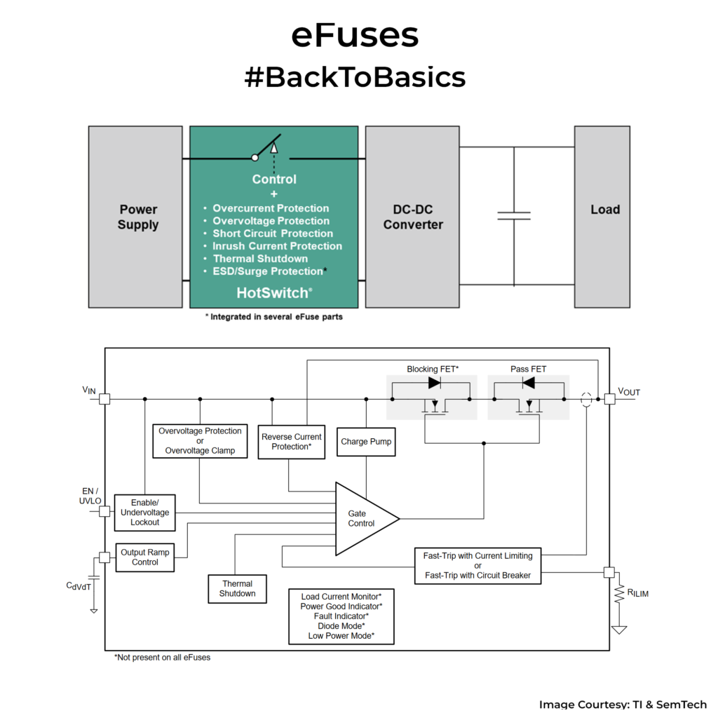
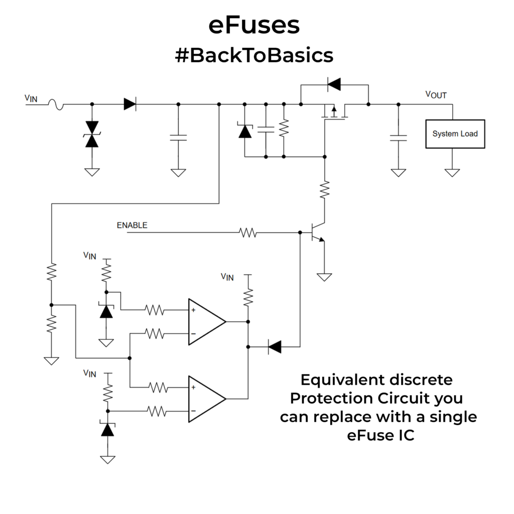
eFuse is an active IC solution with protection features against overcurrent, overvoltage, undervoltage, reverse polarity input, and inrush current. Think of it as an all-in-one solution for circuit protection. Let’s take an example of short circuit protection. Discrete PTC fuses work by changing their resistance when a trip current is hit, but the reaction time is pretty linear and takes time. Meaning that the chances of the circuit going up in smoke are high. Whereas eFuses are much faster to react in these scenarios cutting off power nearly instantaneously(Less than a 1ms!). You need a lot of components to provide the same protection for all the above to even get remotely close to the functionalities of eFuses ie) it takes up circuit space.

eFuses absolutely shine in cases where there are parts that will get plugged in “hot”(Think server parts, SSDs/HDDs, Motors that get pulled in and out while powered on). There will be a huge inrush current trying to charge the decoupling capacitors of the hotplugged device, which can cause voltage droop in the rest of the circuit. This is solved in eFuses by doing a controlled ramp-up of the voltage and current for the circuits it’s protecting. All in all, eFuses are the one-stop solution if you need all these protections. Yes, they are slightly more expensive but worth it when you are protecting high-value components in your circuit.

Have you used them before? Would love to hear about your experience working with them.

If you liked the post, Share it with your friends!

Advanced: Glass Core Substrates

A couple of months ago Intel in an event introduced a cool new tech in the chip packaging domain, which I think is pretty cool. When IC chips get manufactured, they get placed on a substrate which allows chips to talk to other chips. These can be memory, GPU, or with your PC motherboard. The faster you can talk between these units, better the performance. We currently use organic substrates similar to the FR4 materials that you use in your circuit PCBs.


Intel is proposing a new glass core substrate that aims to outperform existing organic substrates, thereby facilitating larger chips on a single substrate. The glass core substrate isn’t an entire glass replacement; it augments the organic material at the core. Metal redistribution layers (RDLs), which allow one part of the chip to talk to another part, are placed on both sides of the glass substrate. The key advantage of glass lies in superior mechanical strength and its being extremely smooth as a surface. Not like the woven fibers in PCBs(Search for microscopic images of your PCB substrate, you can see mountains and valleys). Glass can withstand higher temperatures during packaging and reducing warping. It can transfer data at an extremely high speed with very little losses.

Glass core substrates boast better electrical performance, with Through-Glass Vias (TGVs) similar to your PCB vias but with a very high-density spacing of around 100um between vias. This translates into the ability to accommodate 50% more dies on a chip, a substantial leap in chip density.The transition to glass core substrates will begin later this decade, starting with high-end HPC and AI chips. The limiting factor is its cost. But it’s bound to reduce in price as the tech matures. Likely glass is one of the hottest candidates in the material space. Do check out Project Silica from Microsoft which uses glass to store data for potentially eternal storage of 10,000+ yrs.

If you liked the post, Share it with your friends!
1 3 4 5 6 7 76