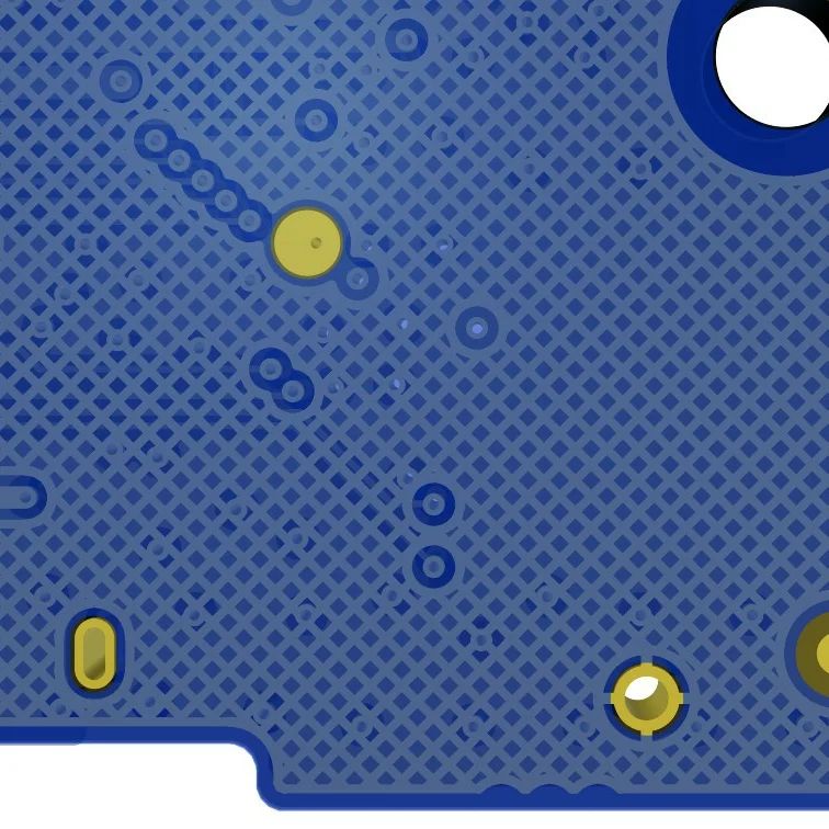
A couple of weeks ago, when I was reviewing a PCB, I found that the designer had given a cross-hatched pattern on one of the outer layers as a return plane on a rigid 2 layer board. When quizzed about it, they mentioned that it was for aesthetic reasons and the cross hatches gave it a cool look. This is all well and good but please understand that the crosshatch ground planes are a thing of the past. Not having a proper ground plane as a return path will affect your high-speed signals.
It came into existence when in the earlier days of PCB manufacturing, manufacturers couldn’t adhere/stick the inner copper layer with the rest of the material prepreg material because the solid copper plane was too smooth. So they had to manually roughen the Solid Cu plane so that rest of the layers would stick. Else there was always a chance of delamination of layers of a PCB. So in order to avoid the manual process, cross-hatching of the plane was done so that rest of the layers can stick properly in between the gaps of the hatch. These days, it’s not a problem anymore with the latest PCB manufacturing techniques. So try to avoid using the cross-hatching as much as possible.
The only reason you would want to use cross-hatching is when you are doing flexible PCBs, the cross-hatching will provide a bit more flexibility to bend for the flex-PCBs. Using solid fills can potentially cause planes to crack.
There is one real edge case though where you would want to use cross-hatched planes, which is to increase the impedance of a controlled line when the layer thickness to the plane below is very small and you need to hit a particular value for impedance. But this is a very hard problem as I haven’t seen any free calculators helping you decide this, you need complex field solvers for that. Most of you would never ever need it. If you need it, you would know for sure.
0 Comments
Comments are closed.