I was recently playing around with ST’s VL53L8CX time-of-flight (ToF) sensor. It sends out 940nm infrared light and measures how long reflections take to return. ST uses two metalenses inside this tiny module, and that sent me down a rabbit hole in optics to figure out what that is.
Think of an ordinary camera lens. Its curved glass or plastic surfaces bend light until it reaches a focus. A metalens can shape light using a surface that is almost flat. Across it sit millions of nanometre-scale pillars, each deliberately sized or shaped.
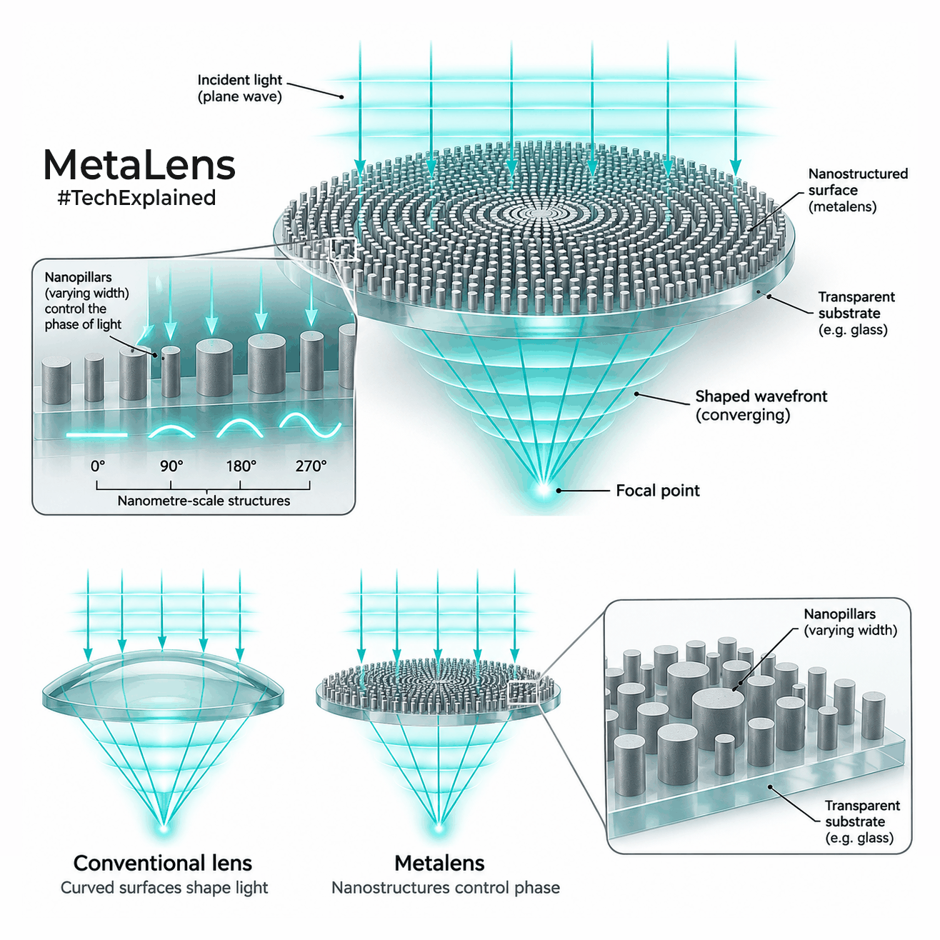
Light really does pass through these structures in common designs. Each pillar changes the phase of the passing light, meaning how that small part of the wave lines up with the rest. Together, they create an outgoing wave that converges at a point, or spreads light into a chosen pattern. That is how a flat surface can perform the job of a curved lens. The pattern can also spread a laser beam into a designed shape, which is useful in sensors.
What are they made from? Usually a transparent substrate, often glass, with patterned materials such as silicon for infrared, or titanium dioxide and silicon nitride for visible light. Manufacturers use chip-making methods like lithography and etching to define the pillars. Nanoimprinting, rather like stamping, can replicate a master pattern for volume production. The patterned layer can be around 1 µm thick.
Applications are limitless. You can make compact optics, shape a laser beam precisely and sometimes replace multiple optical elements. They’re already in depth sensors, facial sensing and other specialised modules. But wide-angle, full-colour cameras are harder. Different colours don’t automatically focus at the same point, efficiency can fall and large areas demand extremely precise manufacturing.
One detail I think is worth keeping in mind: an almost-flat optical layer doesn’t make an entire camera that thin. Light still needs some distance to travel from the lens to the sensor.
0 Comments