A couple of months ago Intel in an event introduced a cool new tech in the chip packaging domain, which I think is pretty cool. When IC chips get manufactured, they get placed on a substrate which allows chips to talk to other chips. These can be memory, GPU, or with your PC motherboard. The faster you can talk between these units, better the performance. We currently use organic substrates similar to the FR4 materials that you use in your circuit PCBs.

Intel is proposing a new glass core substrate that aims to outperform existing organic substrates, thereby facilitating larger chips on a single substrate. The glass core substrate isn’t an entire glass replacement; it augments the organic material at the core. Metal redistribution layers (RDLs), which allow one part of the chip to talk to another part, are placed on both sides of the glass substrate. The key advantage of glass lies in superior mechanical strength and its being extremely smooth as a surface. Not like the woven fibers in PCBs(Search for microscopic images of your PCB substrate, you can see mountains and valleys). Glass can withstand higher temperatures during packaging and reducing warping. It can transfer data at an extremely high speed with very little losses.
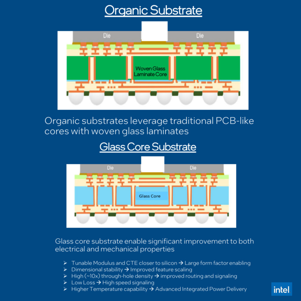
Glass core substrates boast better electrical performance, with Through-Glass Vias (TGVs) similar to your PCB vias but with a very high-density spacing of around 100um between vias. This translates into the ability to accommodate 50% more dies on a chip, a substantial leap in chip density.The transition to glass core substrates will begin later this decade, starting with high-end HPC and AI chips. The limiting factor is its cost. But it’s bound to reduce in price as the tech matures. Likely glass is one of the hottest candidates in the material space. Do check out Project Silica from Microsoft which uses glass to store data for potentially eternal storage of 10,000+ yrs.
0 Comments
Comments are closed.