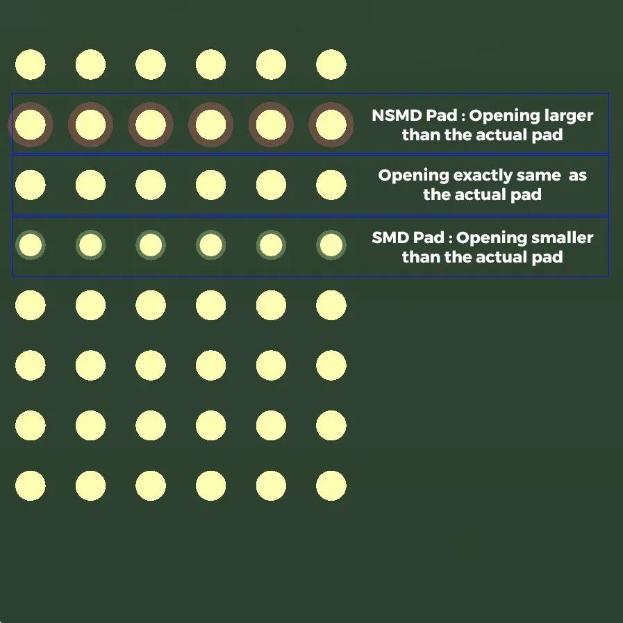
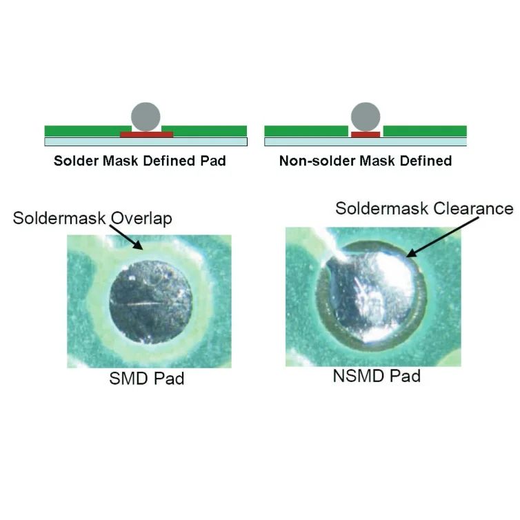
When doing a high-density BGA type PCB routing, you might across these terms. NSMD stands for Non-Solder Mask Defined and SMD for Solder Mask Defined pads. In order to understand the difference, take a look at the image of a 0.4mm Pitch BGA package with 3 selected rows. The first selected row contains NSMD pads, in which the solder mask is removed from an area around the actual physical pad. On the third row, the solder mask opening is smaller and it overlaps the actual pad by some margin. The second row is a compromise where the actual pad size equals the solder mask opening.
Now why are there different ones and what are the pros & cons of each?
NSMD pads are one of the most commonly used ones for large components because it gives the manufacturer a bit more tolerance when they are applying the solder mask layer. In case a slight misalignment happens between the copper layer and solder mask layer in the PCB manufacturing process, having an NSMD pad is beneficial because the pad won’t get hidden under the SM layer as the opening is larger. But these days with a good manufacturer, the chances of misalignment are much lower than before. Now, where does this go bad? Assume you have a BGA part with a pitch(centre to centre spacing between 2 adjacent pads) of 0.4mm or less, now if you have a larger SM opening, you very small width of SM between the pads. That can have a chance of peeling off in the heating/reflow soldering process. Another disadvantage is that you would not be able to route a track between the tracks because the solder balls can potentially bridge to these tracks. The worst-case scenario is that the solder mask width is too thin and the solder balls bridge to an adjacent pad altogether. This might not happen on prototype runs but in large productions, it can affect the yield of the PCBs. Also, another advantage of SMD is that it provides mechanical strength to the PCB pad(the chance of it getting ripped out from the PCB is lesser).
You clearly see that SMD might be preferred over NMSD for smaller pitch parts, but what’s the issue with SMD pads? Since the opening is smaller than the actual pad, for BGA pads you might find that the solder balls might not make full contact with the metal pads as some portion is masked. This can potentially cause mechanical reliability issues wherein the part is not actually soldered properly to the board. Now the other issue is the heat/current transfer. If a pad is designed to carry heat or a particular value of current, reducing the contact area can have issues in the functioning of the part.
So which one to use in your design? As always, it depends on a case-by-case basis. It’s always about balancing your pros and cons. It’s also heavily dependent on how good your manufacturer. Datasheets usually tell you what you need to do. When in doubt and you have no way of taking a decision, follow the datasheet. Keep these in mind for your next high-density design.
PS: I know it’s a slightly advanced post. I tried my best to simplify and explain this, do let me know if you prefer these kinds of posts over normal ones.
0 Comments
Comments are closed.