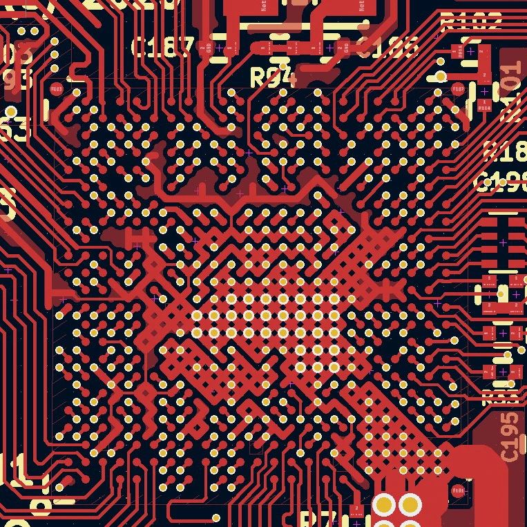
It’s a relatively new PCB manufacturing tech on the market. It is used in ultra-high density PCBs that have a very high premium on space. To understand SAP, first you need to understand the traditional PCB manufacturing process. In a simplified overview, a traditional PCB is made by taking a substrate with Copper already present on it, then you do pattern masking based on the Gerber files that your PCB software provides and then you do chemical etching to remove copper in all areas where PCB tracks and lines are not needed. It’s a subtractive process.
Now the problem with this tech is that since Copper layers are relatively thick, etching away Cu can limit the thickness of the lines. You cant usually go below 3-4mil in thickness of tracks, if you do go thinner, you have the risk of Cu tracks being totally etched away and the track can be broken at places. For very high-density PCBs, designers would want to go below the 3-4mil limit(Think about high pad count BGAs) that’s where SAP shines.
In SAP, rather than taking board with Cu already on it, they start with a substrate. They add pattern masking and do something called as deposit Cu Electroless process. That’s just a fancy way of telling that Cu is deposited on a surface chemically(Not using electricity like electroplating). The advantage of this is that you can create a very thin uniform layer of Cu. Now if you need to remove some parts of Cu so readily do that because your Cu layer is very thin and removes easily. With this tech, you can potentially go to PCB track widths of 1mil(25um) or below.
Since the conventional etching process is not there, you get straight sidewalls(Think in 3D of a PCB trace) with much finer impedance control for those PCB traces(Usual processes may create trapezoidal sidewalls due to over-etching and a has +-10% impedance variation on tracks). This tech is being used by Apple and Samsung in their designs in last 3-4years to make their circuit boards smaller and reduce the layer counts on the PCB. They use something called modified SAP (mSAP) which is a mix of traditional and the new SAP tech(It’s too big to be explained in this post)
0 Comments
Comments are closed.