I thought I should probably do a series on the ubiquitous LEDs in electronics design. You might be thinking what’s there to learn about that? TBH there are a lot more things than you think. Most times when I start embedded hardware interviews, I start with basic LED circuits and how to use them in circuits. Lots of fundamentals to probe there. Surprisingly, even seasoned experts trip up on this area.
At the heart of every LED is a semiconductor chip composed of layers of materials, typically gallium arsenide/phosphide/nitride. When a voltage is applied across these layers, it excites electrons, causing them to jump from the conduction band to the valence band. As they return to their stable state, they release energy in the form of photons, creating visible light. It’s called electroluminescence.
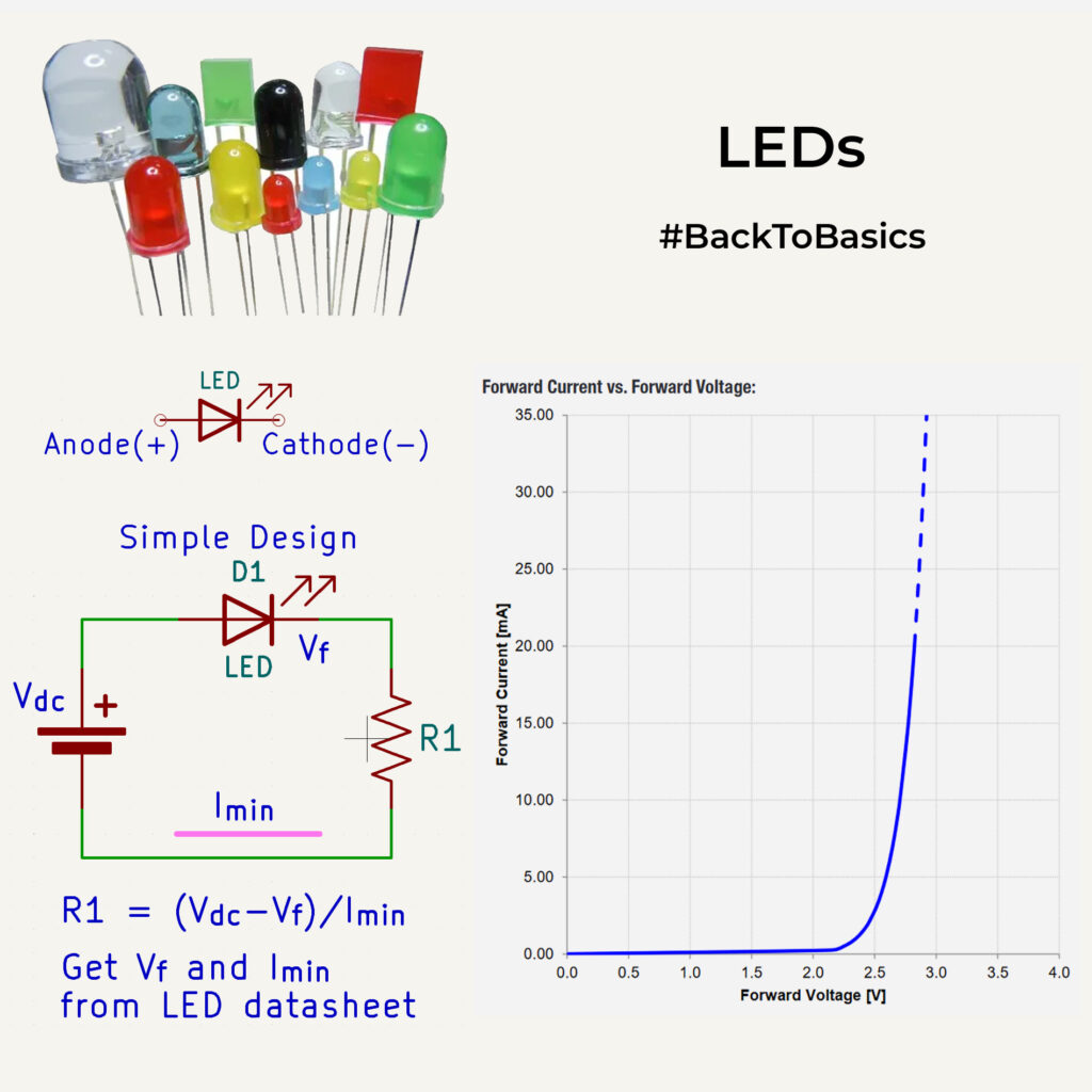
Every LED has forward voltage(Vf) and it changes with color. Everyone knows the exponential IV curve from your first electronics class. LEDs don’t pass current till Vf is reached and then increases drastically. Approx Vf values for diff colours are as follows
Red-1.8- 2.2V
Green/Yellow- 2 – 2.2V
Blue/White- 3 – 3.4V
What you also need to remember is Vf changes(by upto even 20%) even between the same type of LEDs, from the same manufacturer, even from the same batch. Because of this, LEDs are driven with a constant current rather than a constant voltage. Usually more current, more light an LED produces till a point. A very basic LED drive design is there in the pics. It’s our job as circuit designers to ensure what’s the minimum current that needs to pass, to produce the required light output. We will see all about that and more in the upcoming posts.
Feel free to follow or share with a colleague if you believe this series could be valuable, or simply as a helpful refresher.