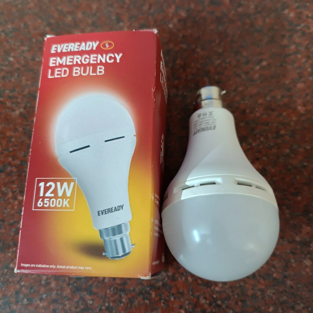
Some of you may have seen these bulbs in your home. At first glance, they seem like your regular LED bulbs, with a string of LEDs powered by AC input. But here’s the twist: they hide a rechargeable battery inside, often an 18650 lithium cell. When the power goes out, this battery springs into action, illuminating a subset of LEDs.
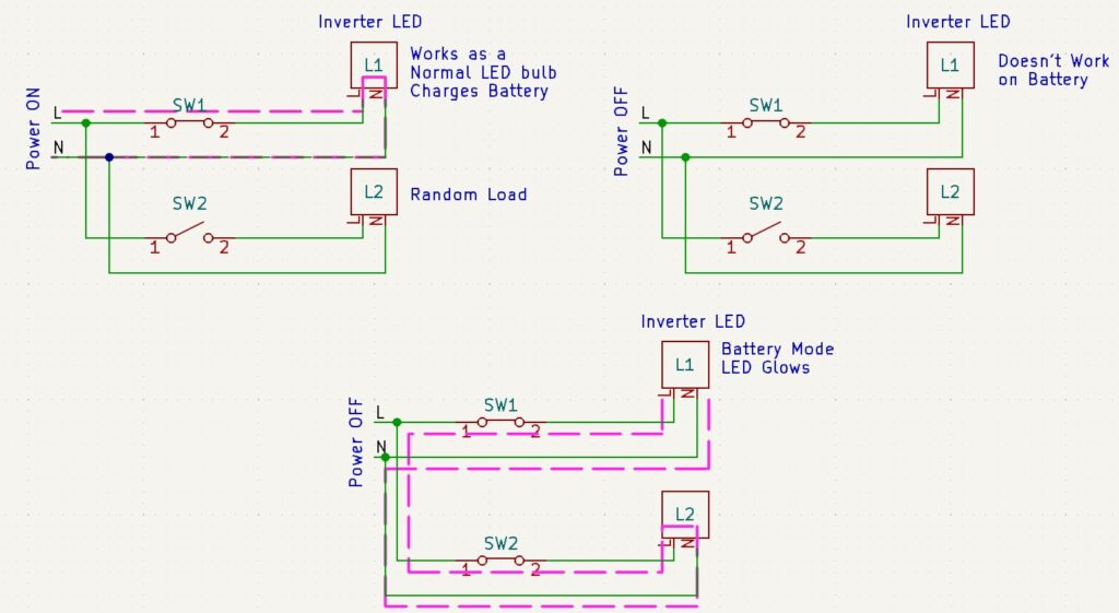
You can get a pretty good idea of what’s packed inside these LED bulbs. It typically includes a standard bridge rectifier and an LED driver for the regular lighting component. There will be a battery charge controller, ensuring the battery gets juiced up during operation. When the power goes out, the battery takes the wheel, supplying power to the LEDs. It’s a straightforward setup, nothing too complex
But here in lies the interesting part, how will the LED know to turn ON when there is no power? Because it can also be that its switch to it is turned OFF. How does it differentiate? It uses a clever mechanism, it can turn ON only when the input AC terminals Live and neutral provide a momentarily closed path. This cannot happen in the normal case and can occur only if another load in the same circuit is also turned ON. It could be any device. This will provide a path for the battery to turn ON power to LED till the actual AC power kicks in.
Consequently, you can perform a seemingly magical feat by merely touching the LEDs with your hands (a reasonable resistance between the AC input pins triggers the battery to power the circuit). It’s a neat party trick that can impress your guests when you effortlessly illuminate an ordinary-looking LED bulb with no external power source, using just your hands! ?