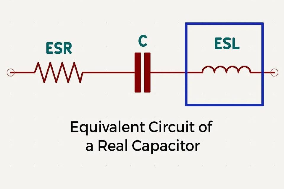
For a real-world capacitor, there are 2 elements worth exploring, ESR(Check older posts to know more about this) and ESL. ESL refers to the inductance that is present in the leads and terminals of a capacitor, as well as any inductance that is present in the capacitor itself. As you see in the equivalent of a capacitor, it’s an RLC circuit, and RLC circuits have a self-resonant freq when the effective inductance and capacitance “cancel” each other and show a minimum impedance. You would have seen those in the V-shaped impedance curves for capacitors. The lowest point of the V shape is the resonant frequency.
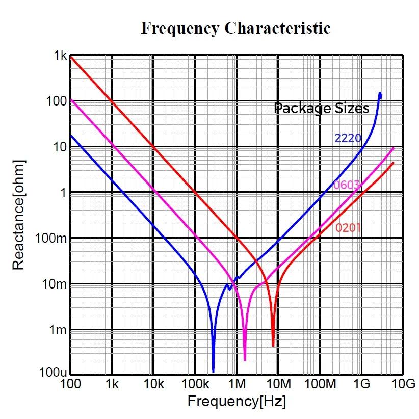
After the resonant frequency, Capacitor doesn’t work like a capacitor. An ideal capacitor is supposed to have a lower impedance for larger frequencies of operation. Xc is inversely proportional to Freq. What we see after the resonant freq in the graph, is due to ESL. The inductance of a capacitor starts dominating and the impedance rises. Now, what’s the problem if impedance rises? Suppose you are using a capacitor beyond the resonant freq in your circuit, impedance seen by your power supply rails will be higher, meaning it will actually resist the flow of high freq components creating noise problems or spikes at the switching instant. Hence we always want to use capacitors with lower ESL in our circuits.
The amount of inductance in a capacitor is primarily influenced by the length of its constituent elements. As the length, or loop area, increases, so does the inductance. Consequently, electrolytic capacitors tend to exhibit significantly higher ESL than their 1206 or 0402 (which is even lower than 1206) counterparts. It is therefore advisable to use the smallest possible footprint size that is compatible with the required voltage rating, in order to minimize ESL. You see that on the graphs, the resonant point shits right and the vertical impedance axis value reduces as you go down in size. Another way to reduce it is to use a flipped capacitor(Check older posts on how they work) with a lesser length.