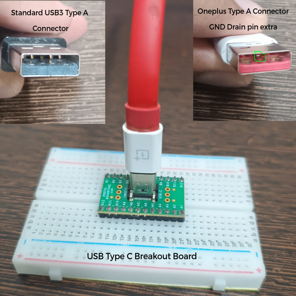
Recently, I misplaced my OnePlus phone’s charging cable and resorted to a Type A to Type C USB3 cable with their original charger. Voila, OnePlus’s superfast charging didn’t kick in with the alternate cable, even though it was of better quality than their official one. This is not a new dilemma; I was curious about how they detect the cable change. Looking at the Type A end of the cable, it appeared similar to a regular USB2.0 Type A connector with the standard four lines: VBus, D+, D-, GND. Interestingly, there was an exposed middle GND-Drain line, which seemed odd. My hunch was that they might be employing some non-standard 1-wire communication over that line.
To delve deeper, I attempted to use a USB TypeC Breakout and probed each pin on the Type C end, but the GND-Drain pin wasn’t connected anywhere. This strongly hinted at the use of an eMarker chip in the cable head. These minuscule chips play a pivotal role in communication between devices and chargers, and that’s where the conundrum arises.
USB Type C cables were intended to establish uniformity and standards, but the industry has managed to turn it into a colossal mess. The market is flooded with seemingly identical Type C cables that differ drastically in performance. And that’s just the physical design part – add to it the proprietary charging protocols introduced by each company. From Apple to Samsung, Qualcomm to Xiaomi, and OnePlus/Oppo, every brand is pushing its unique charging approach, accompanied by flashy names like QuickCharge, Dash/Warp Charge, SuperCharge, and PD fast charging. Just to figure out the Voltage and Current needed.
What’s preventing companies from adhering to a universal standard? The lucrative $50+ billion cable and accessories market. If you purchase a device, you better buy its specific cables or risk a drop in performance due to vendor lock-ins. This issue becomes even more vexing today as companies often exclude chargers and cables when you buy a phone.
This mess won’t be sorted out anytime soon, with USB4 introducing more confusion. Wired cables will be weird in the years to come.