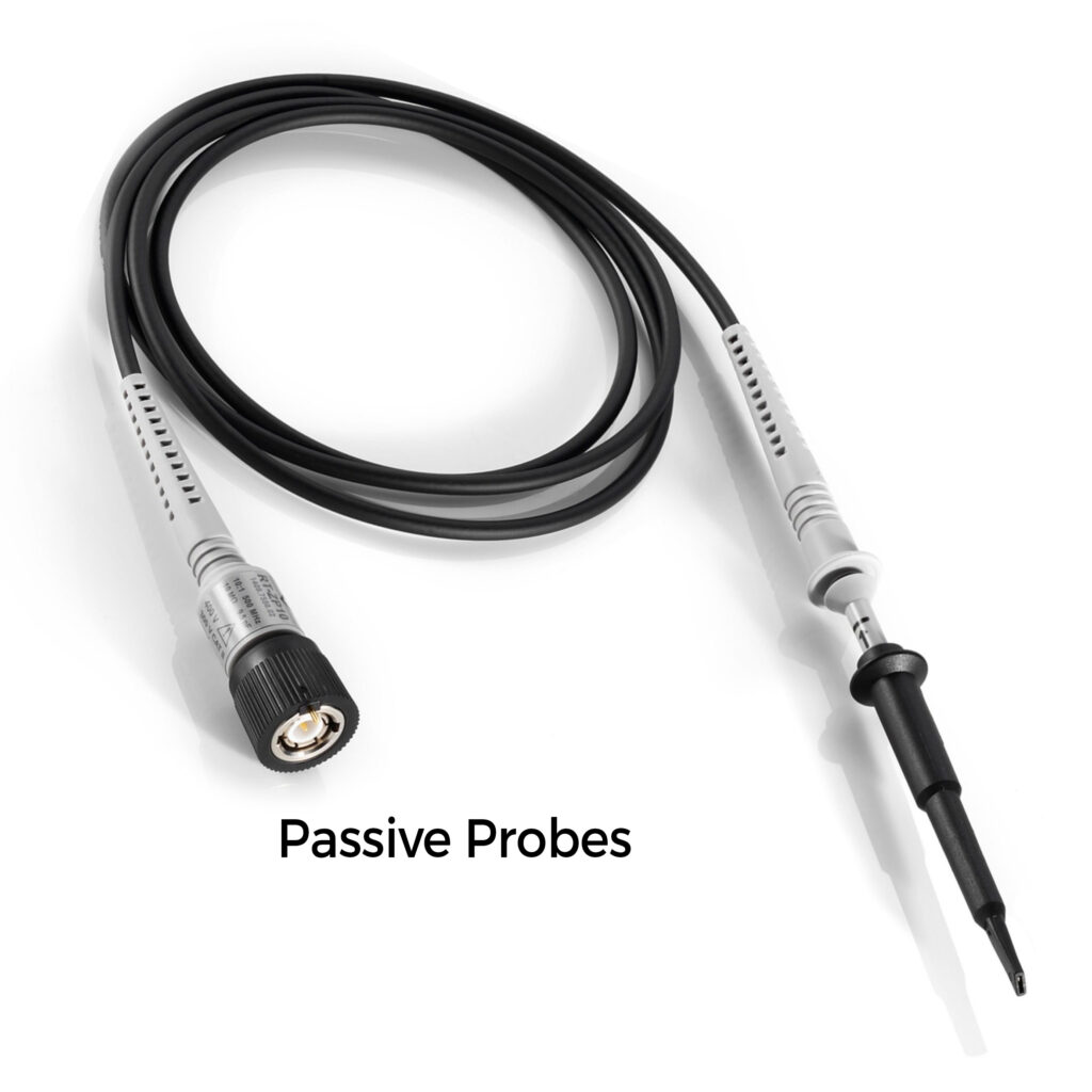
When you start probing(in 10x mode) known signals with higher freq, you will start seeing cases when the oscilloscope is not showing the right amplitude even though the probe is rated for that signal freq & amp. That is due to the fact that your 10x probes are not probe compensated. Let’s delve into what and why?
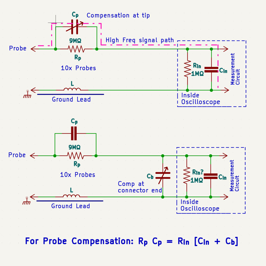
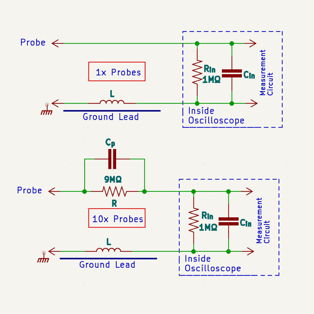
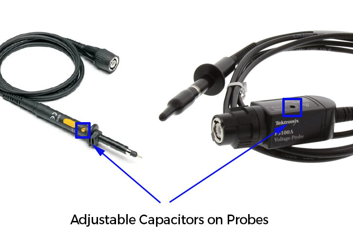
There is always a capacitance(Cin) at the input circuitry inside the scope. It varies between scope models and is usually in the 10pF-20pF range. At higher freq, the impedance of this capacitor drops, if we take a value of 10pF@10MHz (X=1/2*Pi*f*Cin), eff. Impedance is 1.6KΩ only. This low impedance dominates as it is parallel with the 1MΩ at the input and the probe attenuation values go for a toss. Effectively the high freq signal components use the path mentioned in the figure through the tip capacitor. It’s a classic low-pass filter. Whereas the capacitor(Cp) across the 9MΩ is starting to pass high freq signals and is trying to be a high pass filter. In order to fix this, we use a variable capacitor in the probe. It can be placed in 2 spots, one at the tip end and the other at the connector end(Varies in diff models, in some both maybe present). This capacitor is exposed as a tiny knob on the probe which can be rotated to adjust its value. We want the effectively “cancel” out the effects of both RC circuits so that we get flat freq response across the entire range. That is possible only when Rp*Cp = Rin*[Cin + Cb] . This adjustment is called Probe Compensation.
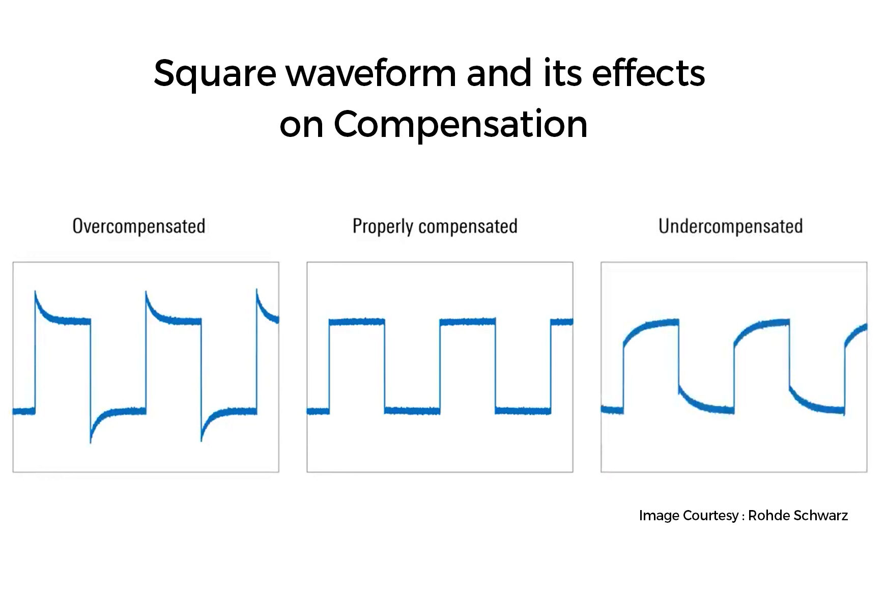
How do you do it in a scope? You connect the probe to a special pin in front of the scope which generates a 1KHz Square wave signal. It’s a square wave becoz it has a low fundamental freq of 1KHz and a sharp rise takes care that high freq components are also present in the signal. Now when you turn the variable cap knob you will see the output waveform changing to undershoot or overshoot. Adjust it just enough to get a perfect square waveform. Probes need to be compensated everytime you change the probe or you change a channel as there will be variations. Do take of that when you probe around next time.