Notice how chargers for laptops and phones are shrinking in size while delivering higher wattage than ever before? One of the key techs behind that is Gallium Nitride(GaN) ICs. GaN has a wider band gap of 3.4 eV compared to Silicon substrates(1.1eV). What this means is that higher energy is needed to move an electron from the valence band to the conduction level for GaN. A wide bandgap allows these devices to work in higher breakdown Electrical fields, higher voltages, and temperatures. Another big difference is in electron Mobility, electrons can move 30% faster in GaN compared to their Silicon counterparts. Which means it can be used for very high-frequency switching applications. This enhanced conductivity also results in improved efficiency since it requires less energy to achieve the same output compared to silicon transistors.
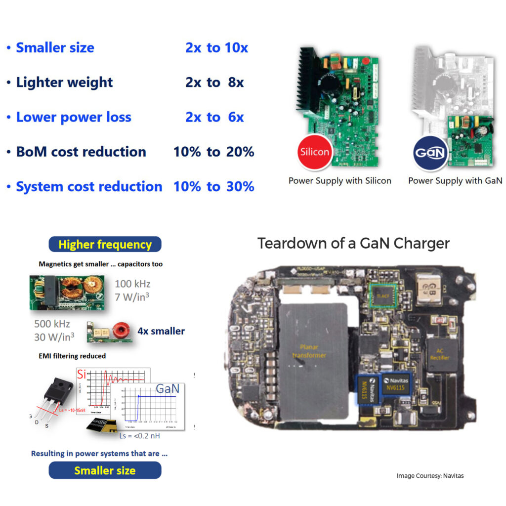
How does all this make your AC to DC charger smaller? The major element in any normal chargers is the transformers which are bulky. They are bulky since they use thicker wires around a core because of the low frequency of operation(50KHz-100KHz range). Now GaN ICs can work at 10x frequency which enables wires to be very thin and even them getting embedded on PCB traces, which enables the bulky transformers to be replaced by planar transformers(A big topic in itself). The higher freq of operation causes a linear scaling down of the size of inductors and capacitors in the design dropping them to tiny SMD ones. Another part you can get away with in GaN is dropping the input EMI filters altogether as the switching losses are minimal. All of these enable a drastic size reduction of the chargers.
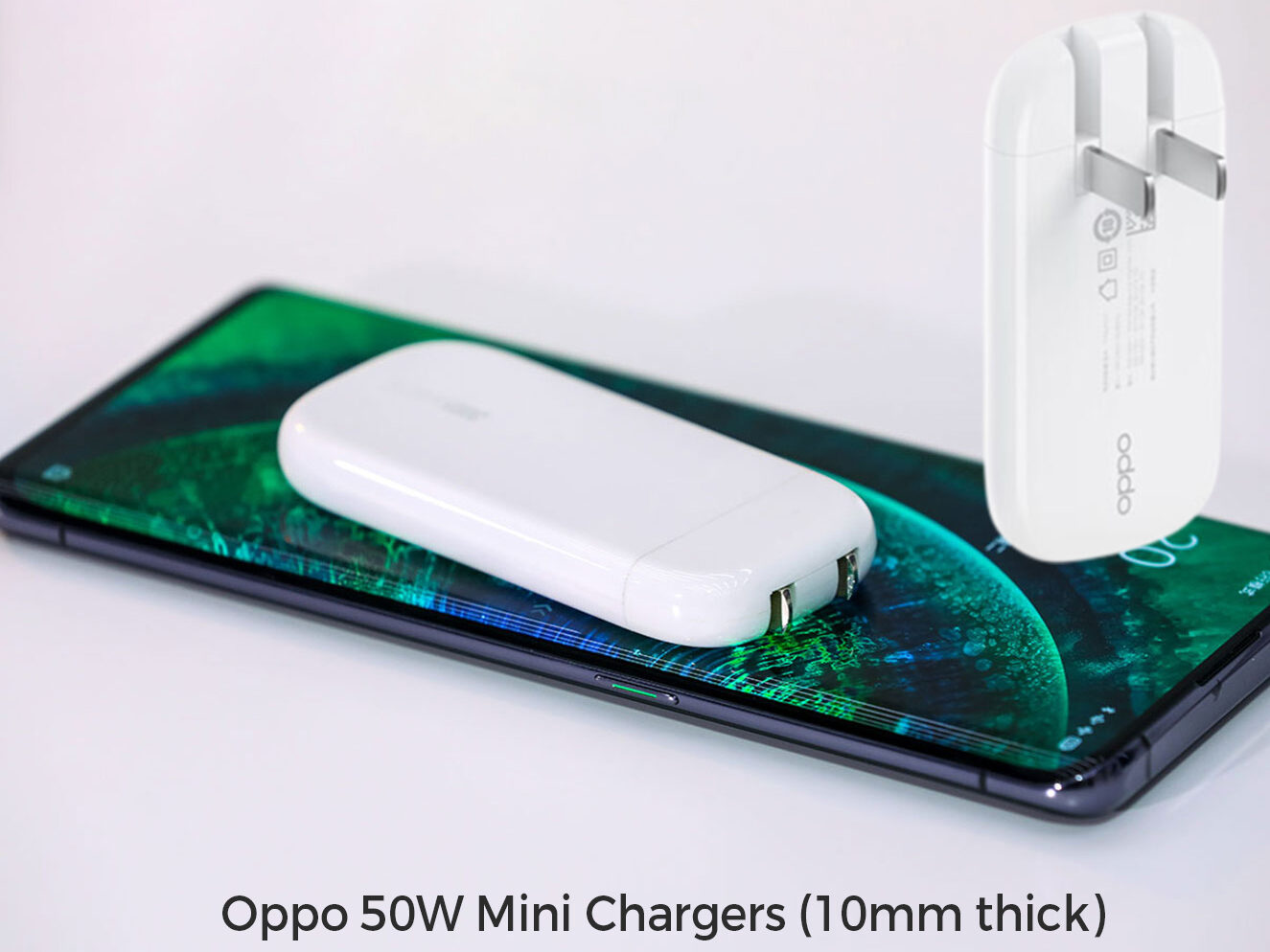
How much reduction is the size? Oppo’s 50W GaN chargers launched 2yrs back is only 10mm thick. Let that sink in. AC to DC conversion at 50W at only a thickness slightly more than the thickness of your phones. There are even higher-powered ones at 300W on extremely small form factors. GaN is definitely the future for power electronics in the sub 500W range.