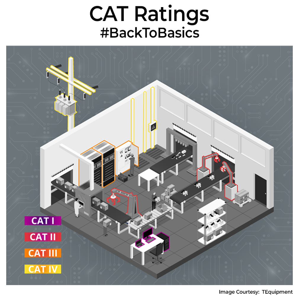
Some of you might have seen these in PCBs. Let’s discuss in detail today.
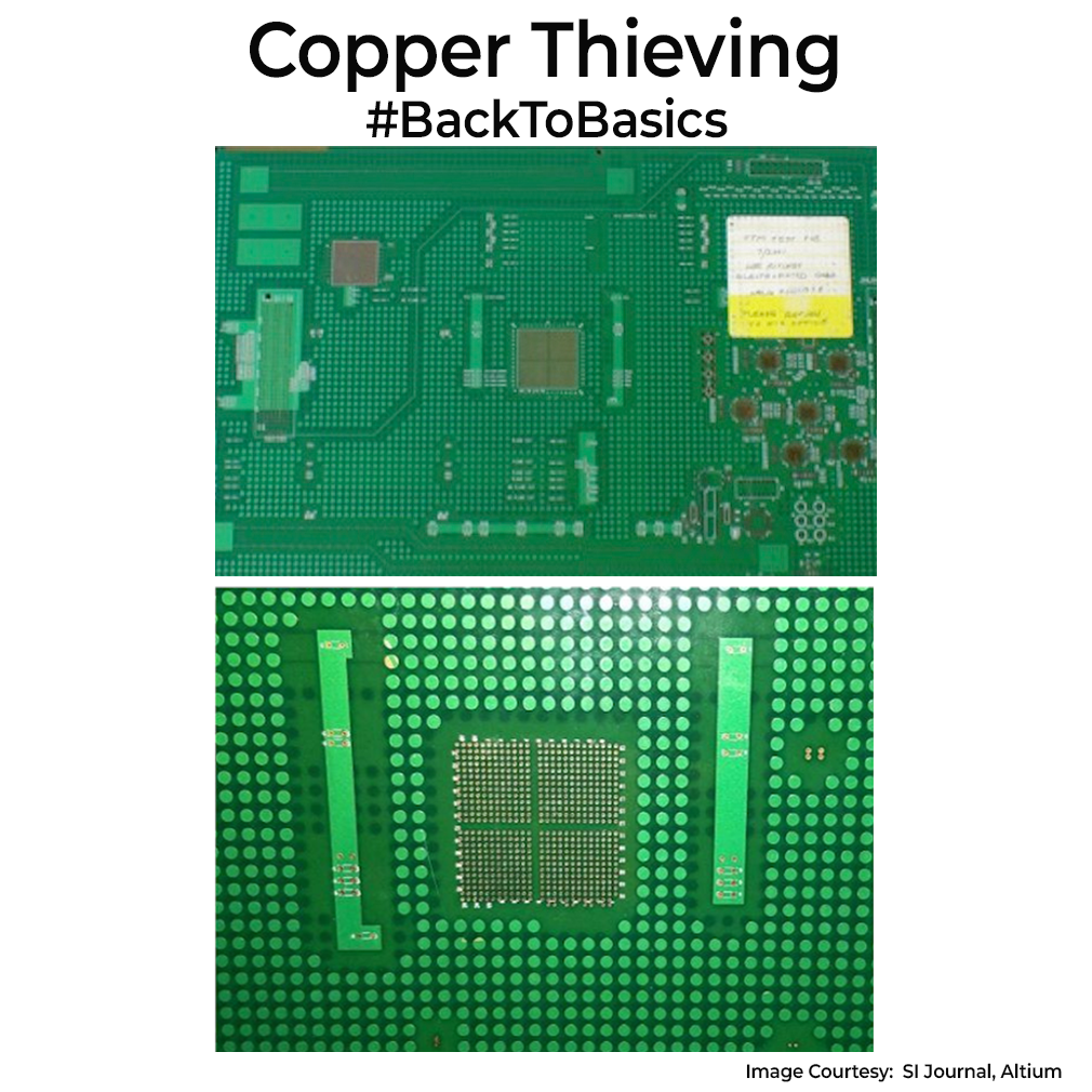
In PCB manufacturing, during the final plating, the bare panel sits in an acid bath and a direct current pushes coats Copper on every exposed metal area on the PCB. Pads, vias and any existing copper act like little magnets. Areas that already have a lot of copper pull harder, empty laminate pulls less. Thick spots get thicker, thin spots remain thin. This is a problem in some cases like the via holes where you will have thickness difference, which in turn can cause signal integrity issues when high speed signals travel through them.
Copper thieving is done to fix this issue. Designers/Manufacturers put small, unconnected dots or rectangles into the blank places on the outer layers of the PCB. These islands are supposed to “steal” a part of the current from certain regions. Current density flattens out, so the whole panel plates at the same pace. This means uniform via walls and traces etch to the correct width/depth.
Do not confuse thieving with copper balancing, though. Balancing is a layout stage move where you mirror large ground pours across all layers so the stack-up expands and cools evenly during lamination and soldering. Thieving lives only on the two plated outer layer (inner layers are etched, not electro-plated). Balancing protects the overall PCB structure and prevents wrapage, while thieving is about fine-tuning in certain surface regions.
If you implement thieving, please remember to keep these islands some distance away from pads/high speed traces or antennas as they are usually not connected to avoid any unwanted coupling. Some folks do connect it to the ground layer with a few vias. So next time when you see some pretty rectangle islands or dots in the design, you will know it’s not there only for making it look nice, they do it to improve the manufacturing yield of PCBs.