Earlier this week I was helping a friend debug a large 5KW inverter circuit which stopped working. In the end, the issue was eventually tracked down to a non-working electrolytic capacitor. Now how do you find a replacement capacitor when dont know the brand? I then realized that it wasn’t common knowledge on how to find out the values of random electrolytic capacitors. This may probably help some of you who didn’t already know. BTW you can’t measure the value with an LCR meter because the capacitor might already be blown. If so, it will just show as an open circuit.
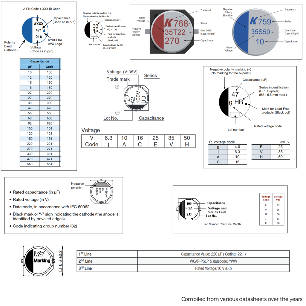
You usually find some weird numbers and characters printed on top of radial cylindrical Can package type electrolytic capacitors. I have collated a list of what those values mean from a few manufacturers in the shared image. It’s pretty self-explanatory from the images. It usually comes in a set of 3 rows from branded vendors. Unbranded ones also do copy and paste these nomenclatures. So there is a high likelihood that you might run into a capacitor with a similar number. Those numbers represent the value, DC voltage rating, temperature rating, and maybe manufacturing code in some. You can save the post/image for some random use case in the future if you ever find yourselves in a spot where you need to replace the electrolytic capacitor on an unknown circuit.
Did you guys ever face this issue before? Or was this something commonly known by everyone?
PS: The Black Line indicates a negative in electrolytic capacitors. Never Ever connect it in the reverse direction. I have learned this the hard way having gotten the part blown to bits. 🙂