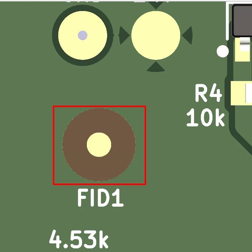
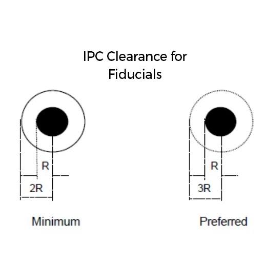
Fiducials are reference marks placed on printed circuit boards (PCBs) during the manufacturing process. They are typically small, circular copper pads that are placed at certain positions in PCB such that the optical alignment systems in the production can use them as a reference point. They are usually used by solder paste dispensing machines and assembly (Pick n Place) machines. It consists of a small circular pad, in which the solder mask is totally removed and the bare PCB substrate is shown. This is done so that optical systems can clearly pick up this spot with maximum contrast. IPC guidelines define that fiducials must be between a minimum of 1mm in diameter or a max of 3mm. The clear area around the fiducial must be at least 1 equal radius as the fiducial mark as shown in the figure.
There are 2 types of fiducials, global and local. Global fiducials are usually placed for large panel boards and are usually placed outside the actual PCB area in the open areas of the panel. They help in getting the overall alignment of the boards correct. Ideally, you need at least 2 points, but 3 or 4 are usually given for redundancy. Local fiducials were usually placed inside a board area to account for rotational alignment for large-size chips and PCBs. But these days, I am seeing that local fiducials are not really used as optical systems have gotten pretty good just aligning with global fiducials. Fiducials do take up space and for every small board, it’s not easy to place local fiducials.
Board houses these days put the global fiducials on the panel and that’s why you don’t see this as a mandate to place it in your design. That doesn’t mean it’s not relevant anymore. If you are designing your own panels for large-scale production definitely make sure you add them.
But never ever put fiducials on the silkscreen layer as a white dot or so. I have seen that in some designs. Fiducials are only to be placed in the Copper layer because Silkscreen layers can shift on the PCB manufacturing cycle between panels during the vertical stack up and alignment.