Gameboy Teardown and Repair

Gameboy
Gameboy Teardown
Gameboy Teardown
Gameboy Teardown
Gameboy Teardown

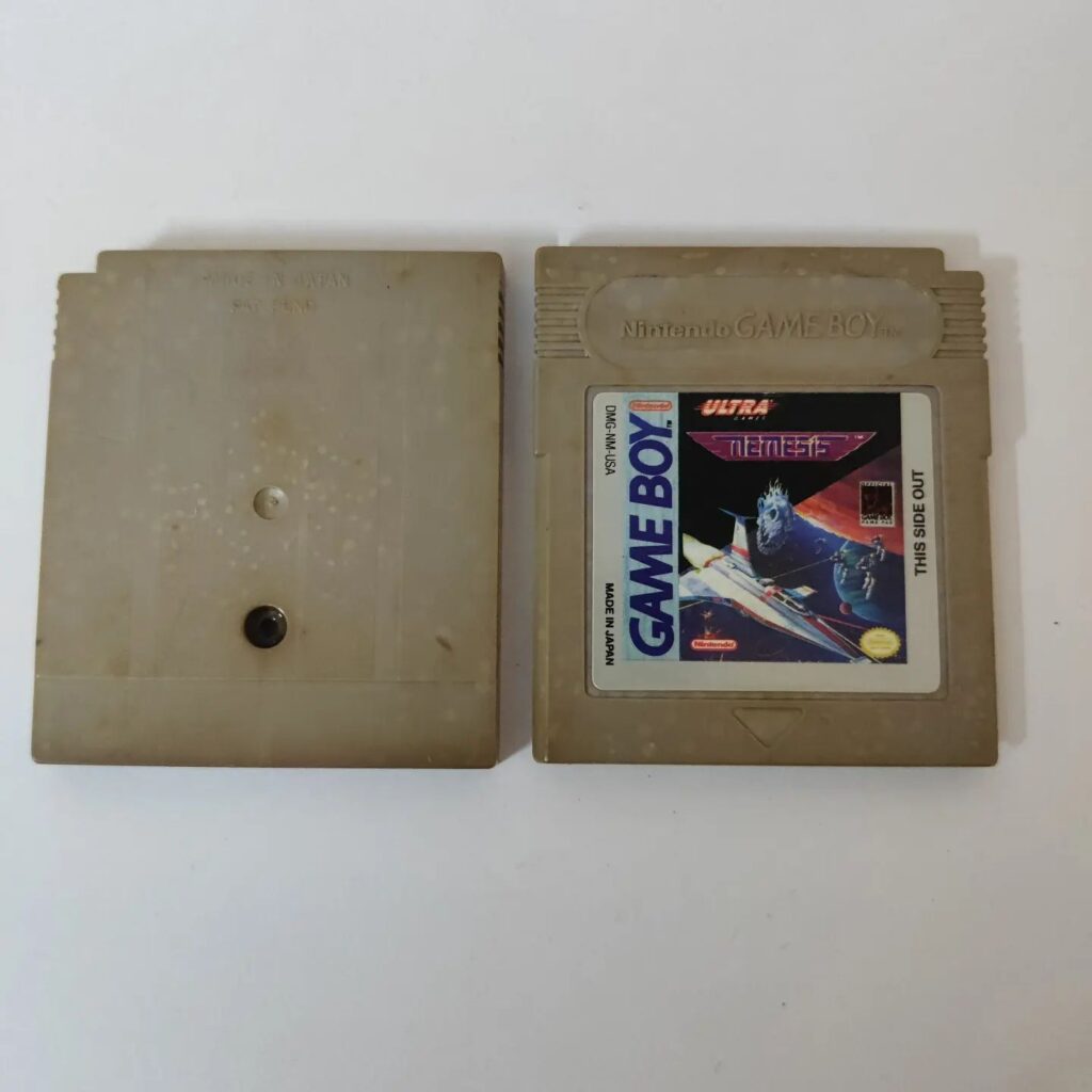
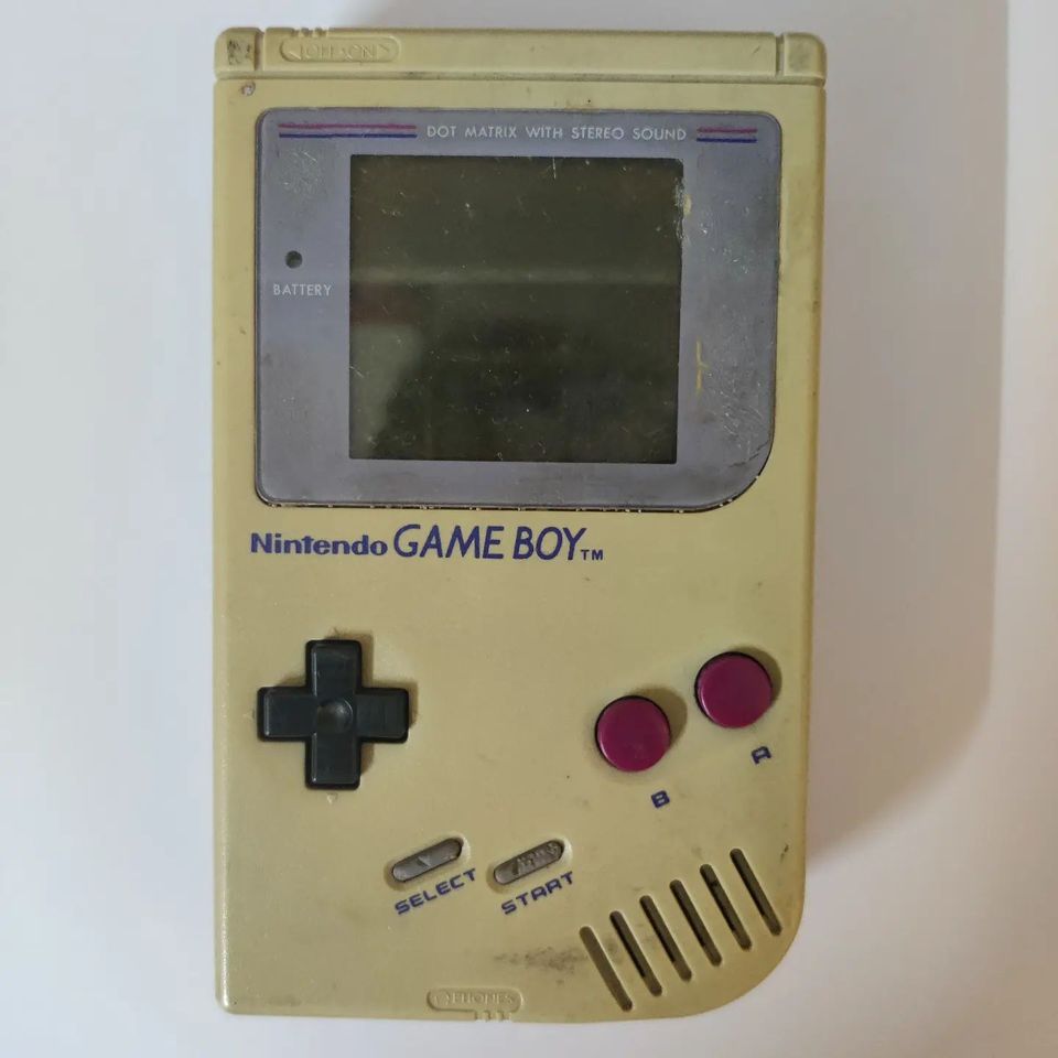
Launched in 1989, it’s probably one of the most iconic handheld game consoles ever created. When I was a kid, I spent quite a few hours playing Tetris and Nemesis(Plane Shooter). This is probably what improved my hand-eye coordination. I found the old Gameboy back home and it refused to turn ON. So thought of doing a teardown and repair.

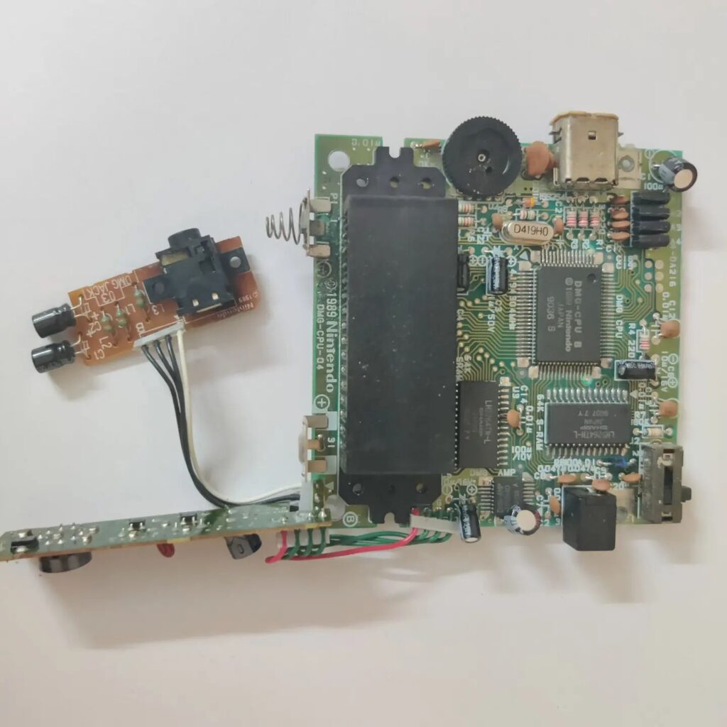
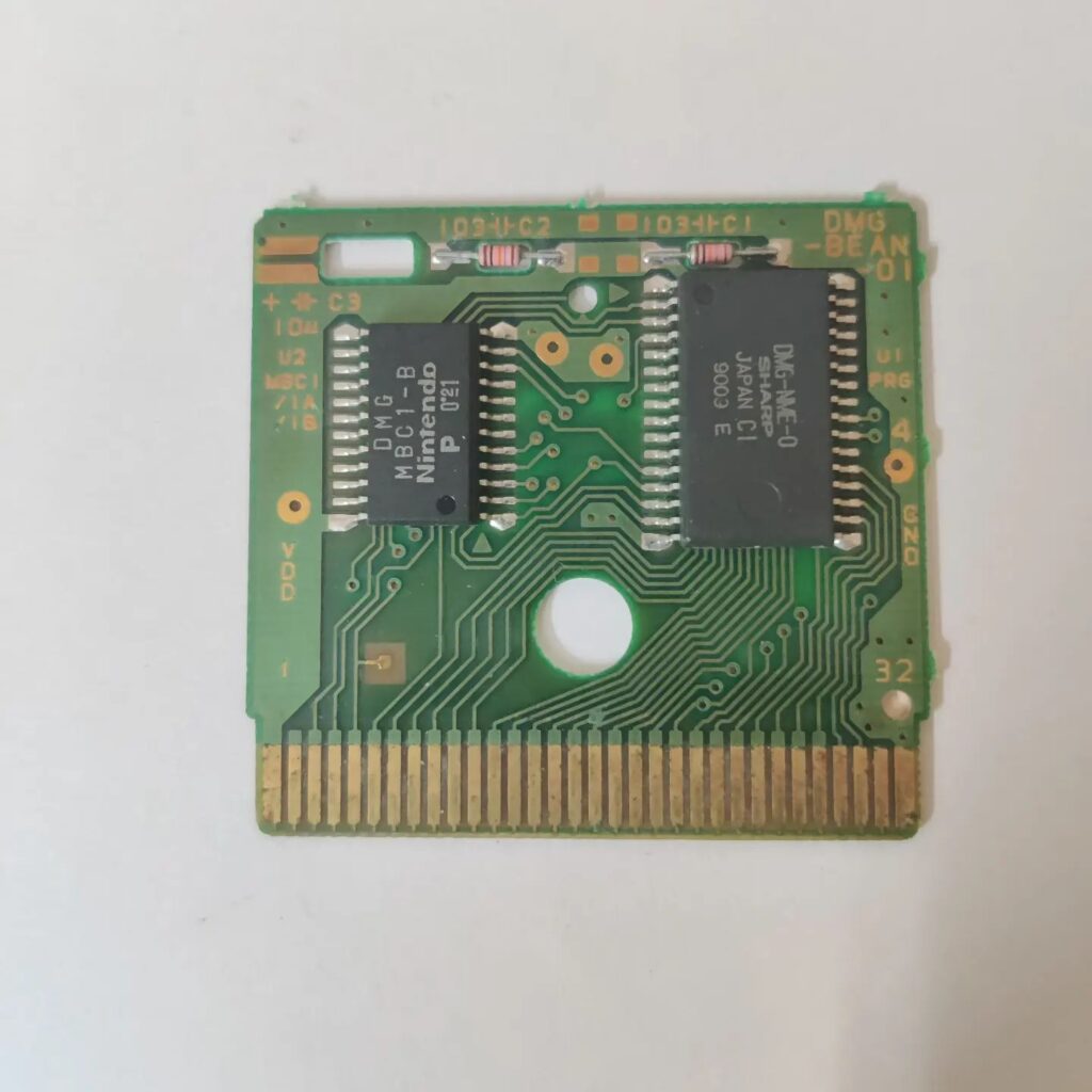
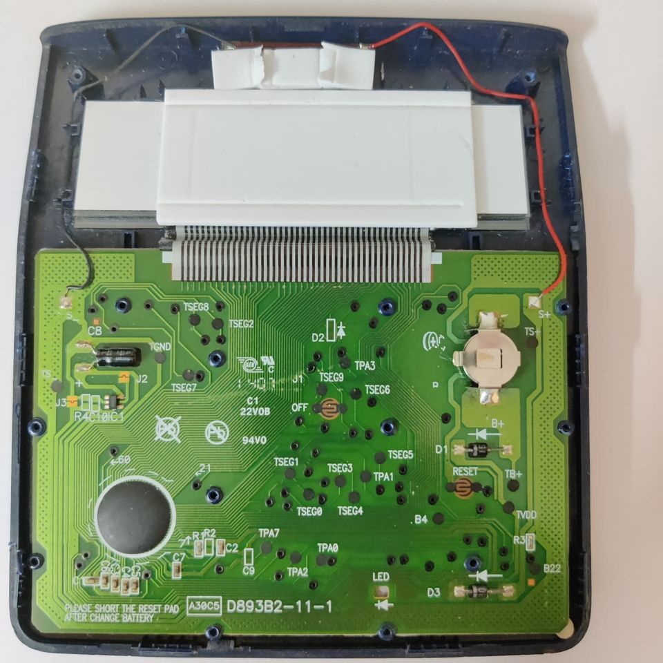
The console contains a custom CPU by Sharp LR35902 clocked at 4MHz. It had 8KB of S-RAM. There is a stereo headphone jack and Piezo speaker for creating those nostalgic Nintendo sounds. The swappable cartridge gets loaded on the back and it communicates via a 32-pin connector. Communicates data via Parallel link with 16bit Address line and 8bit data lane. People over the years have done so many mods on these cartridges to make them even WiFi-enabled with ESP32.

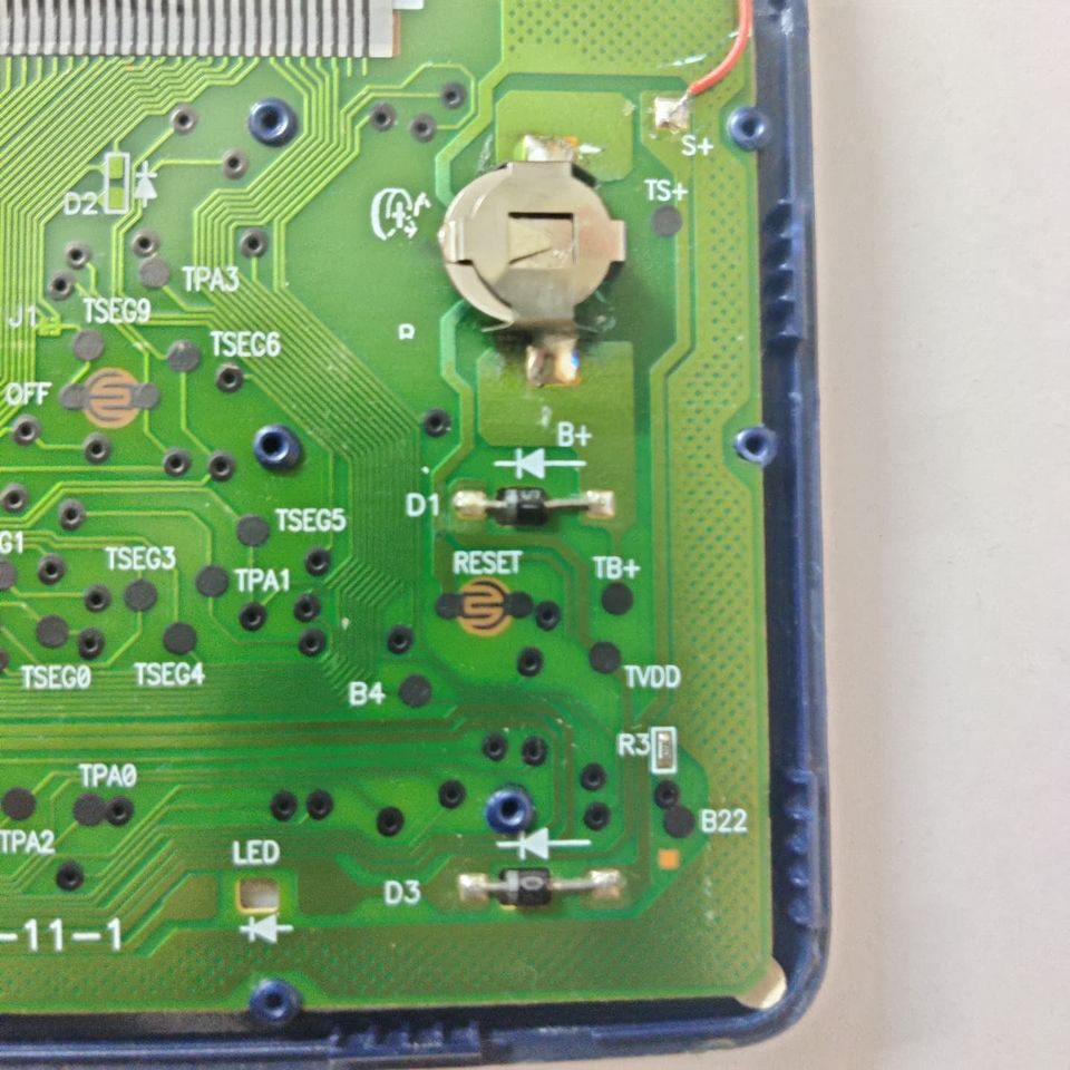
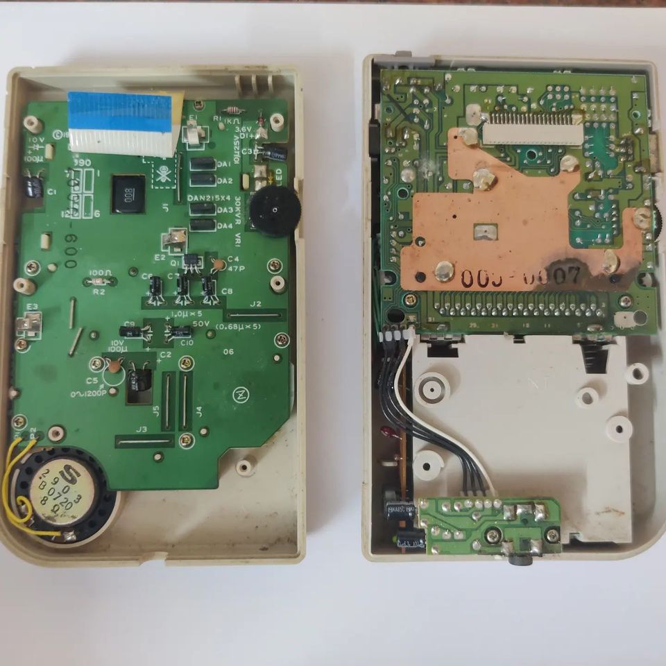
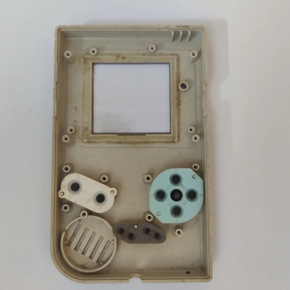
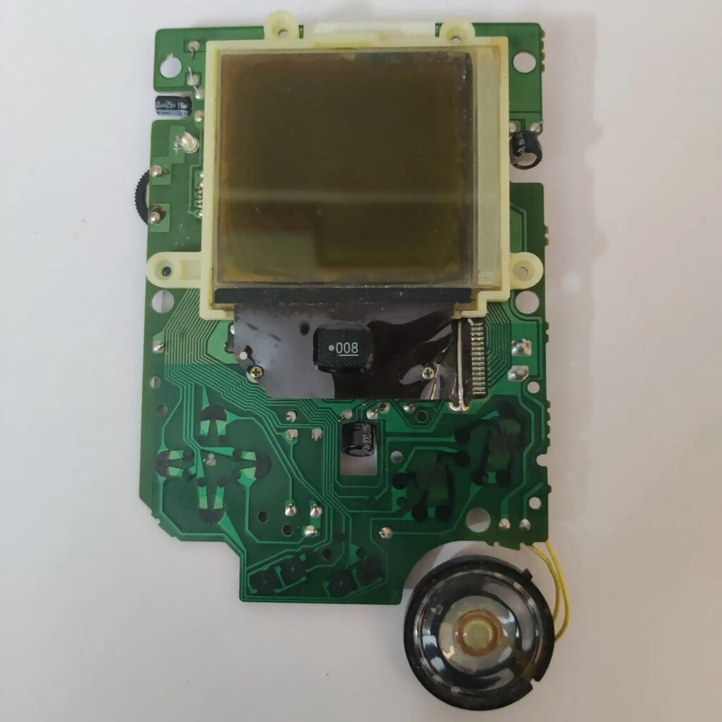
Coming to the repair, It had 30yrs of dust and grime on it. Cleaned out every bit of it, retouched a few solder pads and voila device turns on with iconic Nintendo startup sound. But the display seems to be toasted. Displays on Gameboy’s are based on monochrome Super-twisted nematic LCDs capable of showing 4 shades of olive green. They work by aligning and twisting the Liquid crystal molecules via an electric field. Seems that the crystal layer is damaged and leaked in my unit. This is probably a no-fix till I buy a new replacement screen from AliExpress or so. There seem to a quite a lot of videos on YouTube showing a retrofit IPS display on these Gameboys to create a better high contrast screen. This console might well be one of the most modded/hacked consoles over the years.

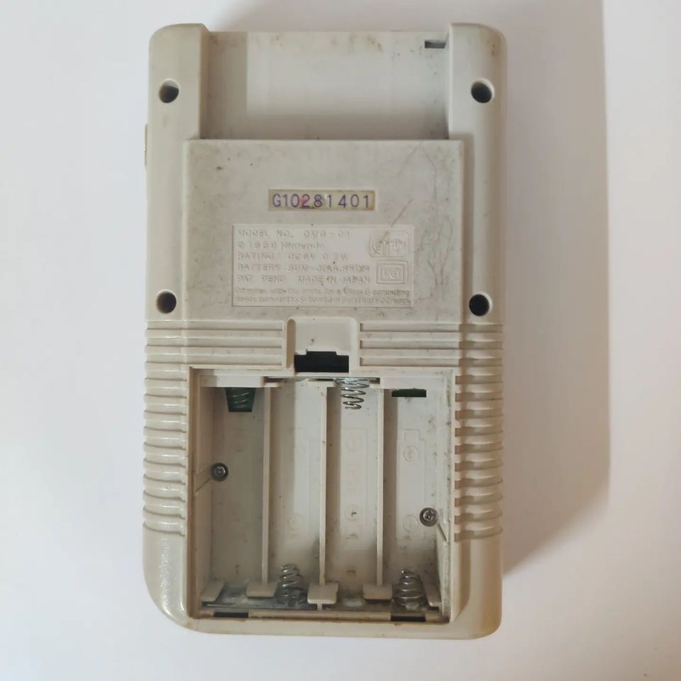
One quirky thing about this unit is that it can be powered externally via a 6V DC barrel power supply(apart from 4 AAs). Since this was released long back, it had the issue that the centre pin was negative(which is not a norm these days). So be careful trying to power these with the latest DC power supplies. Make sure polarities are proper.

Gameboy Teardown
Gameboy Teardown
Gameboy Teardown
If you liked the post, Share it with your friends!

Casio MJ1200 Calculator Teardown

Pocket calculators are a classic example of something which has been around since the 1970s and has undergone optimised design over the years. These still do have a place in the world despite the touch-based software phone calculators out there. The tactile button press feedback is something that a heavy user will always appreciate.

Casio Calculator Teardown

The basic building blocks of a calculator will be your power source, a matrix keypad, an array of 7 segment LCDs and an ASIC(on a black blob) built for cost. The matrix keypad will be a standard row-column arrangement with multiplexing being used to read out the button presses. The button would consist of a carbon-coated unit with a zig-zag portion on the PCB which will effectively make a short with carbon when pressed. The 7 segment LCDs are monochrome and mostly reflective based. Since most calculators don’t carry a backlight they are quite low power to drive(One of the reasons why calculator batteries seem to last forever). The LCD segment is connected by a ribbon cable which is usually glued in place in a PCB(Not soldered) with carbon tracks. If you ever see certain segments in a calculator not lighting up, try heating the cable connector on the PCB end, it should mostly work.

The power section of these calculators usually contains an alkaline button cell battery(1.5V, Not rechargeable). Most of the calculators come with a solar cell array to act as a dual power source. This one had 4 solar cells with a total open voltage of approx 2.5V. It uses the classic power OR-ing circuit. Both battery and solar cells feed into the same PCB track with individual Schottky diodes(Parallel). So solar does contribute to the longevity of the calculator’s battery life. The Schottky diodes in the circuit prevent the reverse charging of the battery and have a low dropout of approx 0.15V. It’s the cheapest possible arrangement based on BOM costing for powering the device. That 0.15V drop is OK for low power circuits like these but won’t scale for larger circuits and hence most IC companies make a killing with power path management ICs these days (Well that’s a discussion for another day entirely)

If you liked the post, Share it with your friends!
1 10 11 12 13 14 20