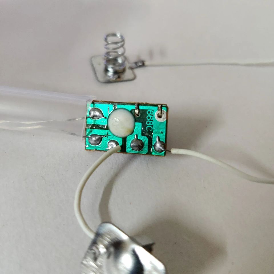
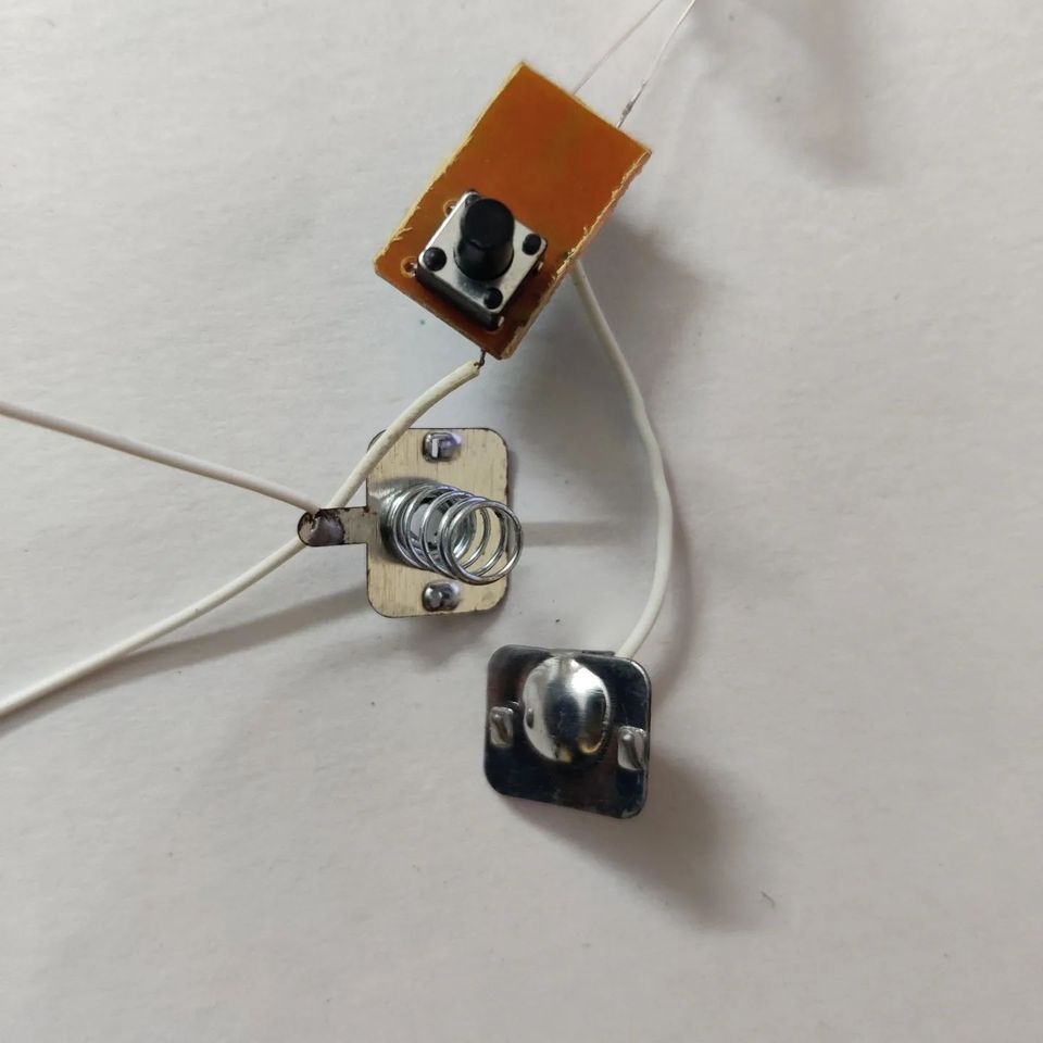
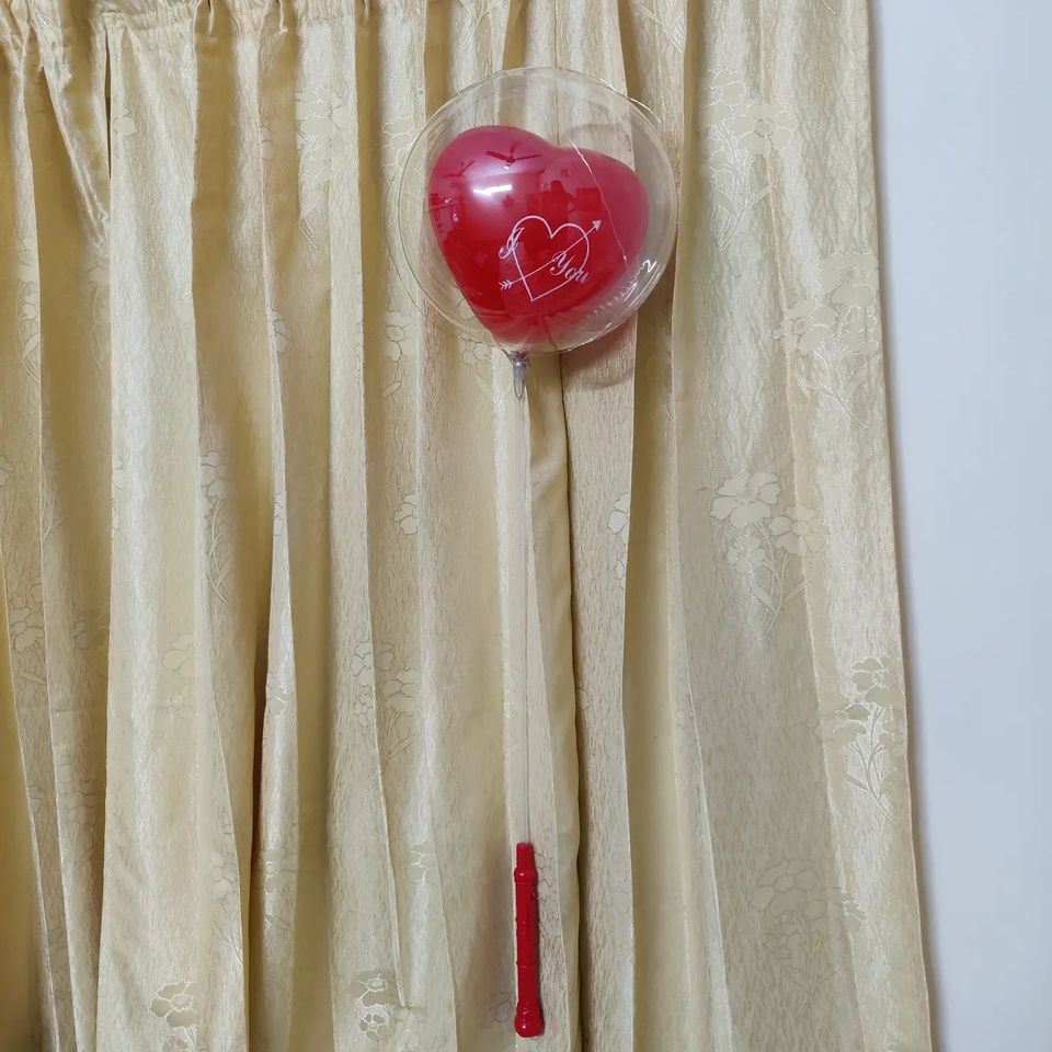
I have written about similar toys and lights earlier too, but toys these days outdo all possible ways of cost-effectiveness. What you see in pics and videos for this post are fancy light balloon lights. These are available on the roadside for INR 50($0.6) but cost less than INR 20 ($0.25) to manufacture. Just take a moment to think about how ridiculous that price is. For INR 20, you get 2 high-quality medium thickness balloons, 28 LEDs, 3AA Batteries, a PCB with an ASIC LED driver, a push-button switch, 3m long single-stranded 26AWG wire, 2 battery spring contacts, 3 injection-moulded hard plastic handle pieces, long flexible plastic tube and a plastic ring to hold everything in place. How crazy is that? That’s the power of Chinese manufacturing at scale. You can say whatever you want about the geopolitical situation, folks from China do know how to manufacture electronic stuff, period. Just imagine how you might solder 28 LEDs on a bare wire, at least that would amount to some cost. How on earth is this so cheap?
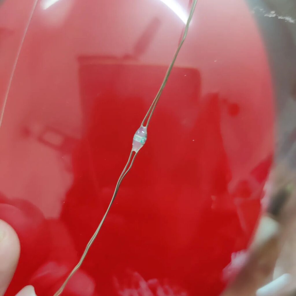
Coming to the electronics teardown, all that the PCB contains are the leads for the battery, a push button connected to a custom ASIC LED driver with 28 LEDs(each of a single colour type) all connected in parallel on an approx 3m wire. The push-button cycles through 3 modes(PWM drive) of LED blinking operation on the sequential presses of the button and finally turns OFF. I measured the power consumption of the circuit. On steady-state mode consumes approximately 60mA of current amounting to 2mA/LED. On the blinking states, it’s around 35mA in total. Considering the total price, the custom ASIC will be costing INR 2-3. That’s insane. It’s always fun to figure out how these toys are put together.