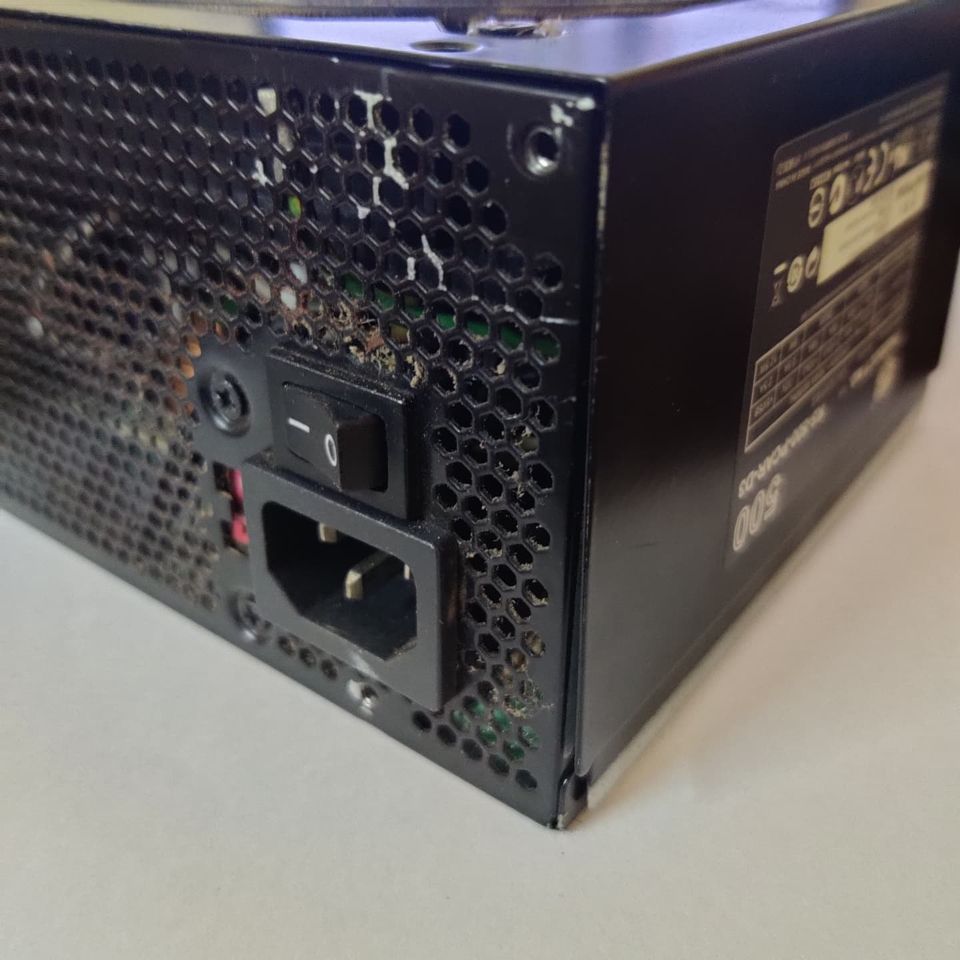
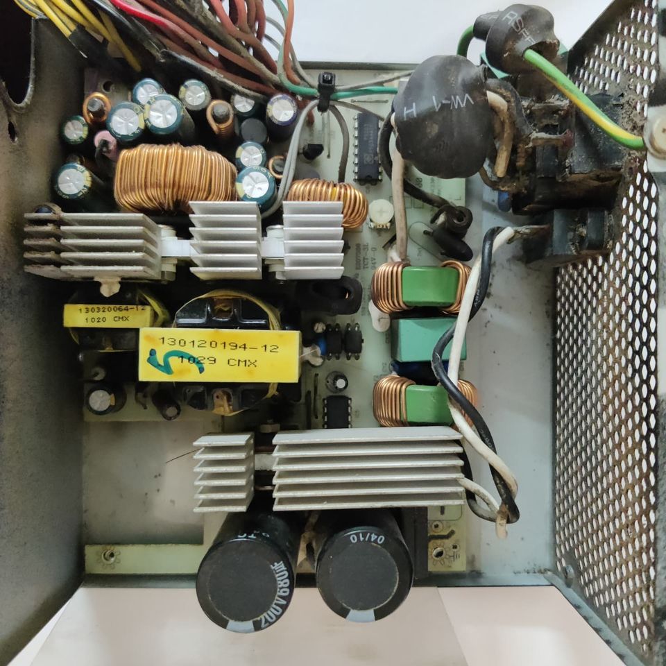
These beefy mountable power supply units power up custom-built desktop PCs. It’s one of those mass-manufactured switched-mode power supplies which are optimised for the cost, in any fashion possible, even from the branded companies. Images show a teardown of 500W Cooler Master PSU. Usual building blocks of a PSU like this contain the input AC filtering section(To remove noise from input and to avoid coupling noise from the power supply back to the main AC supply) made up of fuses, MOVs(Over voltage protection), common mode chokes and huge power line filters. These filtered AC gets fed to bridge rectifiers to convert it into DC and is followed by massive DC bulk capacitors(Be very careful while handling these as it can give you a good shock if you touch their leads before discharging).
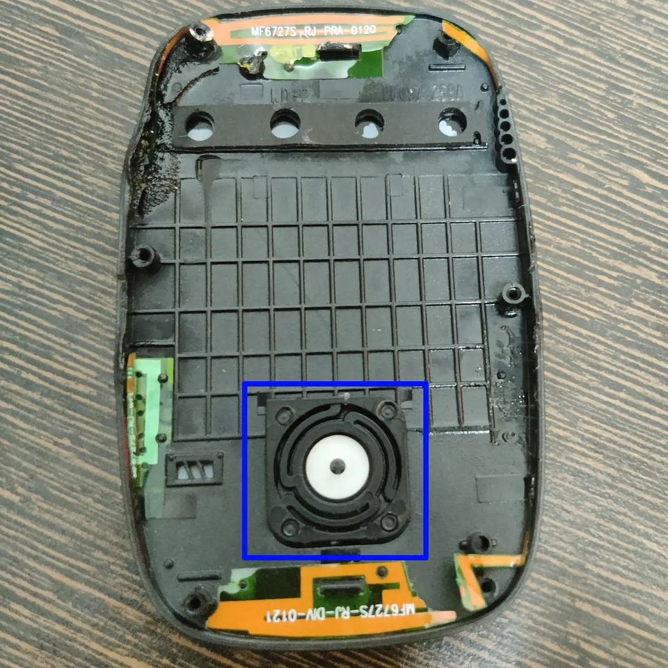
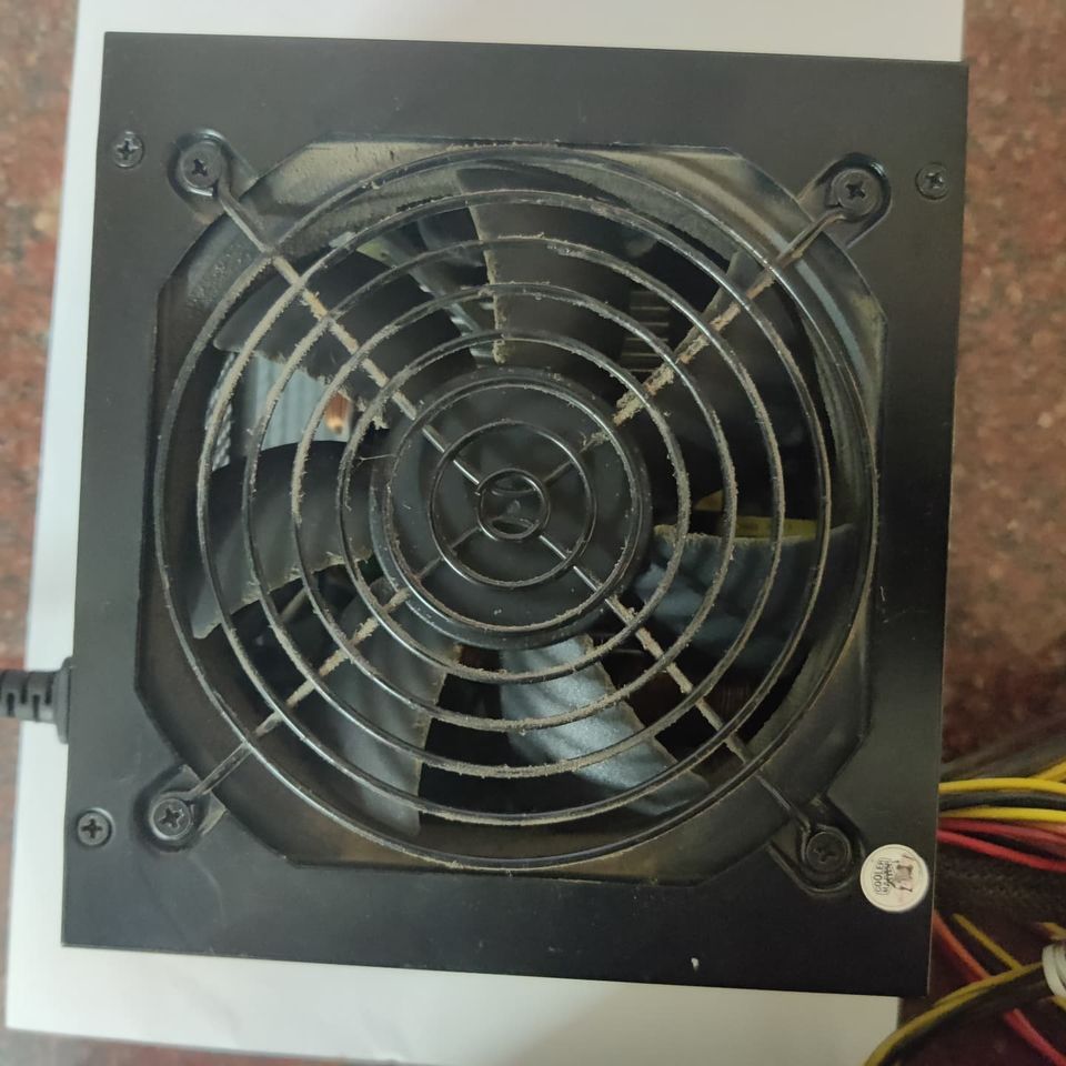
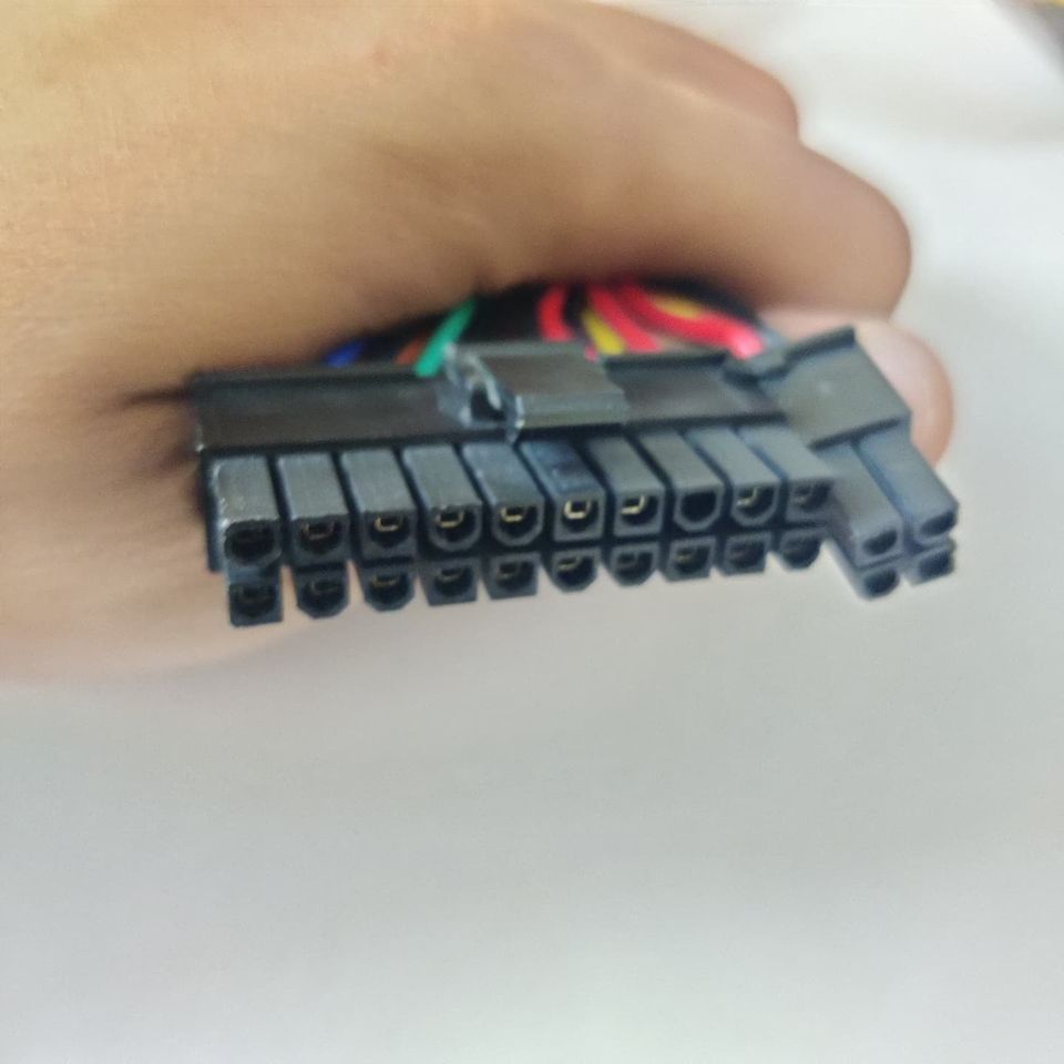
The output DC is fed to switching MOSFETs which chop it up to high-frequency pulses to drive the large transformers. The switched-mode section would contain a feedback back loop to regulate the voltage to desired levels. The output side, based on the ATX standards, provides voltages to different portions of a motherboard. Standard voltage levels would be +3.3V, +5V, 12V, -12V(For RS232 signalling) and is broken out as a 24pin(20+4) ATX connector with a standard pinout. The output side would contain a protection IC for overvoltage, undervoltage and overcurrent to safeguard the motherboard. A fan is provided to cool down the heat produced in switching MOSFETs(to ensure long life).
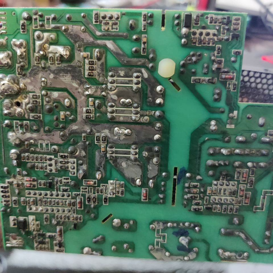
The funny part about the PCB layout of an ATX power supply is that it’s usually one-sided(Ignoring the rule of thumb to the fact of having ground layers and close return paths) purely for cost reasons. The PCBs are usually of a lighter colour and more importantly, made of FR2 Phenolic Resin(Not the usual FR4) because they are cheaper. Hence these units are an engineering marvel in themselves to pass standards and keep the pricing down.
PS: I have been away for a month from my regular posts since I lost someone very close to me. Was not in a great mental space the last few weeks to share posts. Things are getting back to normal and posts would be mostly regular from now on.