Teardown: 7 Port Active USB3.2 Hub

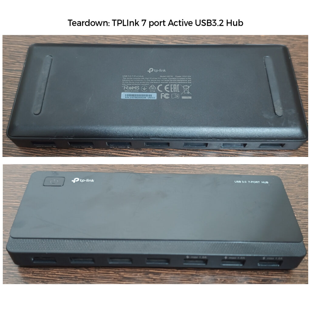
Haven’t done a teardown in a while. Had a TP-Link UH700 7-port USB hub in my scrap pile(But it was working). It’s a 12V powered USB3 hub with 7 ports and Micro USB3 input. After a solid 15-minute struggle, I managed to pry it open – those clips were tough! Needed multiple spudgers for the job.

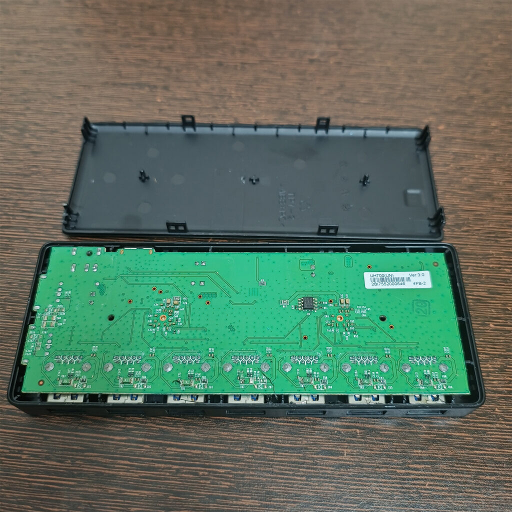
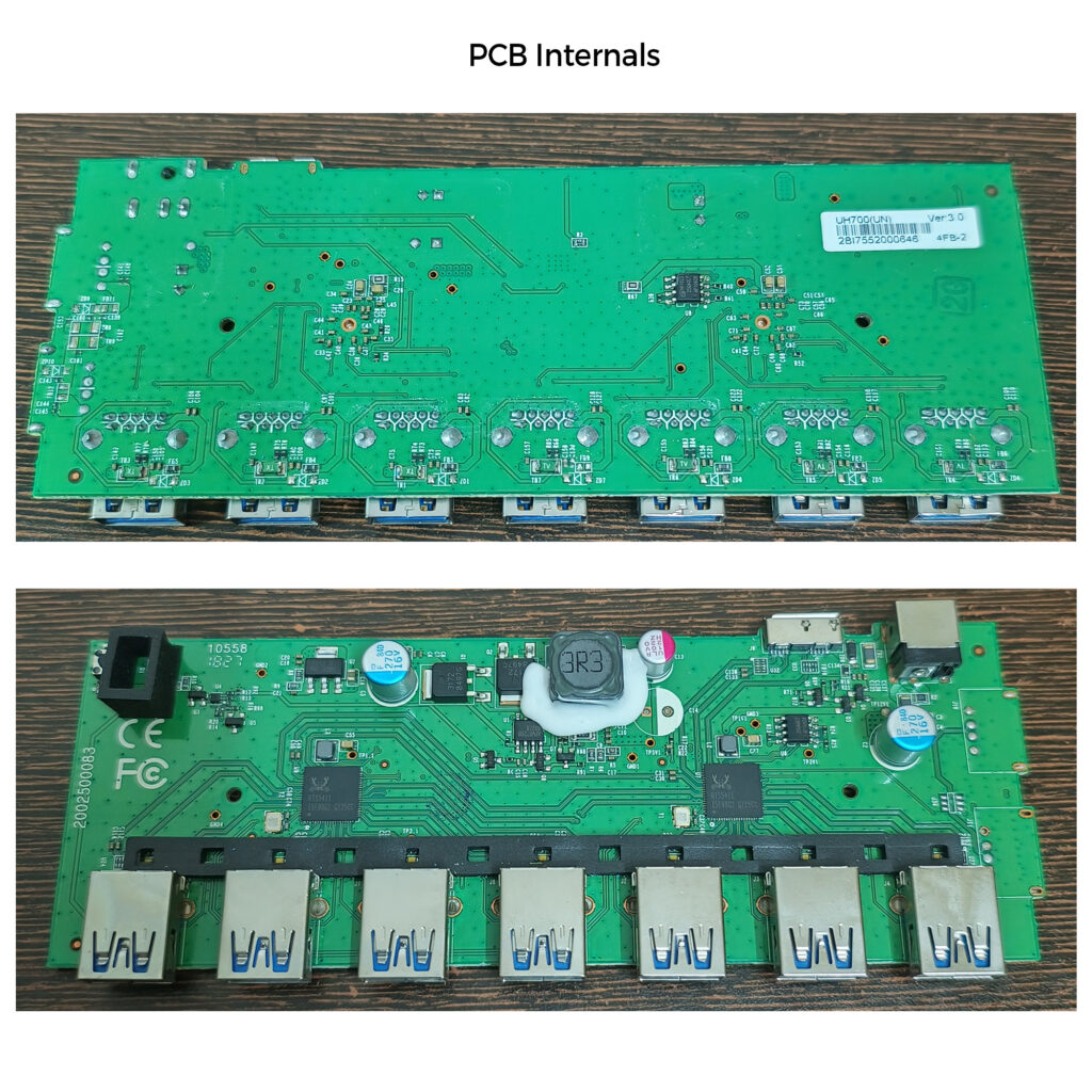
Coming to the internals, the star of the show is two RTS5411S USB3.2 Gen1 4-port Hub controllers(In the middle row) powering 7 ports with a 12MHz crystal. The 8th port is routed as an input to the second RTS5411S. Firmware configuration likely resides in 25Q40CT SPI serial NOR flash chips located on both sides of the PCB. A convenient soft latch button rests on the top left. The power section on the top right and middle contains a 12V input jack and step-down buck converter APW8720B to put 5V through to beefy N-channel MOSFETs CED3172 and a massive inductor at the output. This chip fuels downstream 5V supply and an adjustable 1117 LDO supports the 3.3V rail. Each of the 7 ports has a PTC fuse protection to avoid blowing up if one port draws more current. There is a single LED to show if a port is active and the good part is that LEDs are optically isolated with a cheapo(but effective) black foam. There seems to be space for 2 more USB2.0 charging ports on the right which I believe is for a different Hub model with the PCB. Use the same PCB and sell it as a 9-port device. More Profit.

What’s intriguing is that every port has a footprint for an ESD diode array, yet none of the 8 USB ports, including the input port, have been populated. This seems like a risky approach and a strict no-no in my books. My assumption is that TP-Link might have used these chips on the certification test board to pass tests but omitted them in production to cut BOM costs. Though against the rules, this is a practice I’ve seen before in consumer products from other companies too. These units are likely to struggle with ESD tests. Has anyone in low-humidity environments faced ESD problems with this model?

If you liked the post, Share it with your friends!

Advanced: GaN Devices and why they make your chargers small

GaN Chargers High Speed

Notice how chargers for laptops and phones are shrinking in size while delivering higher wattage than ever before? One of the key techs behind that is Gallium Nitride(GaN) ICs. GaN has a wider band gap of 3.4 eV compared to Silicon substrates(1.1eV). What this means is that higher energy is needed to move an electron from the valence band to the conduction level for GaN. A wide bandgap allows these devices to work in higher breakdown Electrical fields, higher voltages, and temperatures. Another big difference is in electron Mobility, electrons can move 30% faster in GaN compared to their Silicon counterparts. Which means it can be used for very high-frequency switching applications. This enhanced conductivity also results in improved efficiency since it requires less energy to achieve the same output compared to silicon transistors.

GAN Charger Teardown

How does all this make your AC to DC charger smaller? The major element in any normal chargers is the transformers which are bulky. They are bulky since they use thicker wires around a core because of the low frequency of operation(50KHz-100KHz range). Now GaN ICs can work at 10x frequency which enables wires to be very thin and even them getting embedded on PCB traces, which enables the bulky transformers to be replaced by planar transformers(A big topic in itself). The higher freq of operation causes a linear scaling down of the size of inductors and capacitors in the design dropping them to tiny SMD ones. Another part you can get away with in GaN is dropping the input EMI filters altogether as the switching losses are minimal. All of these enable a drastic size reduction of the chargers.

How much reduction is the size? Oppo’s 50W GaN chargers launched 2yrs back is only 10mm thick. Let that sink in. AC to DC conversion at 50W at only a thickness slightly more than the thickness of your phones. There are even higher-powered ones at 300W on extremely small form factors. GaN is definitely the future for power electronics in the sub 500W range.

If you liked the post, Share it with your friends!
1 2 3 4 5 20