Advanced Tech: BYD Battery Cells

I was doing some deep dive research into latest EV cell tech and wanted to learn more on BYD Blade Cells. It’s a nice bit of tech.
It’s a long, slim rectangular can, approx 1m in length, made of lithium-iron-phosphate(LFP) chemistry. As its LFP chemistry, energy density is slightly lower, but it does give longer number of charge cycles. A single Blade holds 135Ah and about 432Wh(160Wh/Kg). For perspective, Tesla’s cylindrical 4680 cell(much smaller though) carries just over 23Ah @ 86Wh, but at a higher 241 Wh/kg thanks to its nickel based NMC811 chemistry. LFP gives around 3000 charge cycles, compared to 2000-2500 for NMC811.

BYD Battery

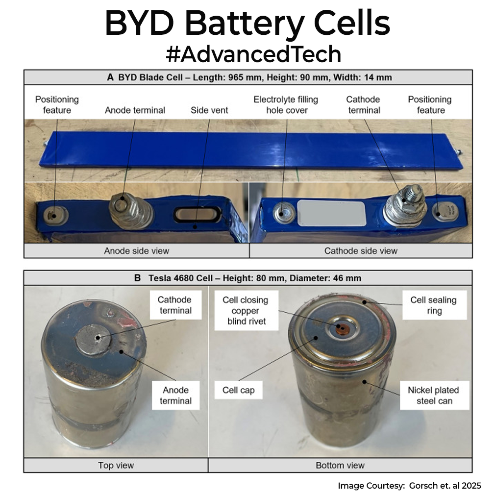
BYD folds its electrodes in a Z pattern, laying the layers flat along the length of the can. That geometry shortens current paths, so the cell can rely on simple dual-side bus bars instead of hundreds of welded tabs like Tesla, who rolls its electrodes into a spiral and cuts thousands of tiny virtual tabs along the edges to spread current evenly. 4680 cell puts out more than twice the heat than a Blade cell. BYD cell’s DC resistance is round 60 mΩ, much lower than a typical 4680’s 80–100 mΩ.

A paper from Gorsch et al. puts BYD cell BOM around €62 per kWh, roughly €10 cheaper than the 4680. This delta scales up to significant savings in high-volume production. In a pack, thin water-glycol plates slide between Blade cells, reducing coolant volume by up to 30 percent.

Reg. Pros and Cons. Blade wins on cost, safety, ease of pack cooling and even repair. Single cells can be replaced easily, unlike fully potted 4680 modules, improving serviceability and reducing warranty costs. It loses out on volumetric energy density though, so long-range or high-performance vehicles still lean toward the 4680. Simulations show one blade cell alone can absorb about 18% of a side-impact’s energy before the pack frame even steps in. So it’s quietly acting as part of the car’s crash structure. I think Blade cells are a winner for urban and commercial EVs.

PS: BYD’s battery volume in 2024 was over 150GWh, that’s over a whopping 300 million cells. They are here to stay for sure.

If you liked the post, Share it with your friends!

Back to Basics: Copper Thieving

Some of you might have seen these in PCBs. Let’s discuss in detail today.

Copper Thieving

In PCB manufacturing, during the final plating, the bare panel sits in an acid bath and a direct current pushes coats Copper on every exposed metal area on the PCB. Pads, vias and any existing copper act like little magnets. Areas that already have a lot of copper pull harder, empty laminate pulls less. Thick spots get thicker, thin spots remain thin. This is a problem in some cases like the via holes where you will have thickness difference, which in turn can cause signal integrity issues when high speed signals travel through them.

Copper thieving is done to fix this issue. Designers/Manufacturers put small, unconnected dots or rectangles into the blank places on the outer layers of the PCB. These islands are supposed to “steal” a part of the current from certain regions. Current density flattens out, so the whole panel plates at the same pace. This means uniform via walls and traces etch to the correct width/depth.

Do not confuse thieving with copper balancing, though. Balancing is a layout stage move where you mirror large ground pours across all layers so the stack-up expands and cools evenly during lamination and soldering. Thieving lives only on the two plated outer layer (inner layers are etched, not electro-plated). Balancing protects the overall PCB structure and prevents wrapage, while thieving is about fine-tuning in certain surface regions.

If you implement thieving, please remember to keep these islands some distance away from pads/high speed traces or antennas as they are usually not connected to avoid any unwanted coupling. Some folks do connect it to the ground layer with a few vias. So next time when you see some pretty rectangle islands or dots in the design, you will know it’s not there only for making it look nice, they do it to improve the manufacturing yield of PCBs.

If you liked the post, Share it with your friends!
1 12 13 14 15 16 93