These are one of the fundamental communication standards out there for sending data between devices. RS stands for “Recommended Standard”. In its simple terms, RS 232 is used for point-to-point communication between 2 devices. You have RX, TX line and you share a GND line between the devices. Its main limitation is the speed of transmission and how immune it is to noise signals. They can do max 1Mbps and can extend the distance to around 15m.
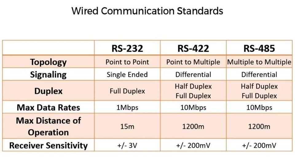
RS422 was introduced to remove the shortcomings of RS232. It supports single-point to multiple-receiver connections. Meaning you can broadcast information. To improve noise immunity, they use a differential pair. So you have just 2 wires running between systems for a half-duplex connection and 4 wires if you want a full duplex. So effectively you have a higher bandwidth (Around 10Mbps) and you can have a longer cabling length of 1000m+. It uses twisted pair lines with a termination of 120 ohms.
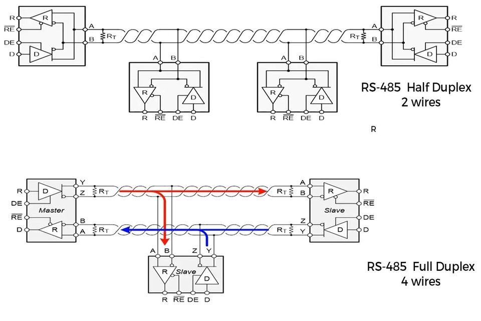
RS485 is again an improvement over RS422 wherein electrical standards remain the same but it introduces the concept of multiple transmitters and receivers in a single line. For RS485, on the driver end, you need to have a minimal differential of 1.5V between lines whereas on the receiver end the differential is 200mV so you do have a large margin for longer transmission of signals. As usual, longer the distance, lower the speed of transmission you can achieve.
It is imperative to understand that, all the above three are electrical standards and not protocols(Protocols define how data is packed and sent) or connector types. It tells you the signal amplitudes, how it can be wired, termination resistance etc but not how to transmit data over it over a signalling scheme. These standards are still in use because it’s cheaper to implement for lower bandwidth wired data transmission between systems.