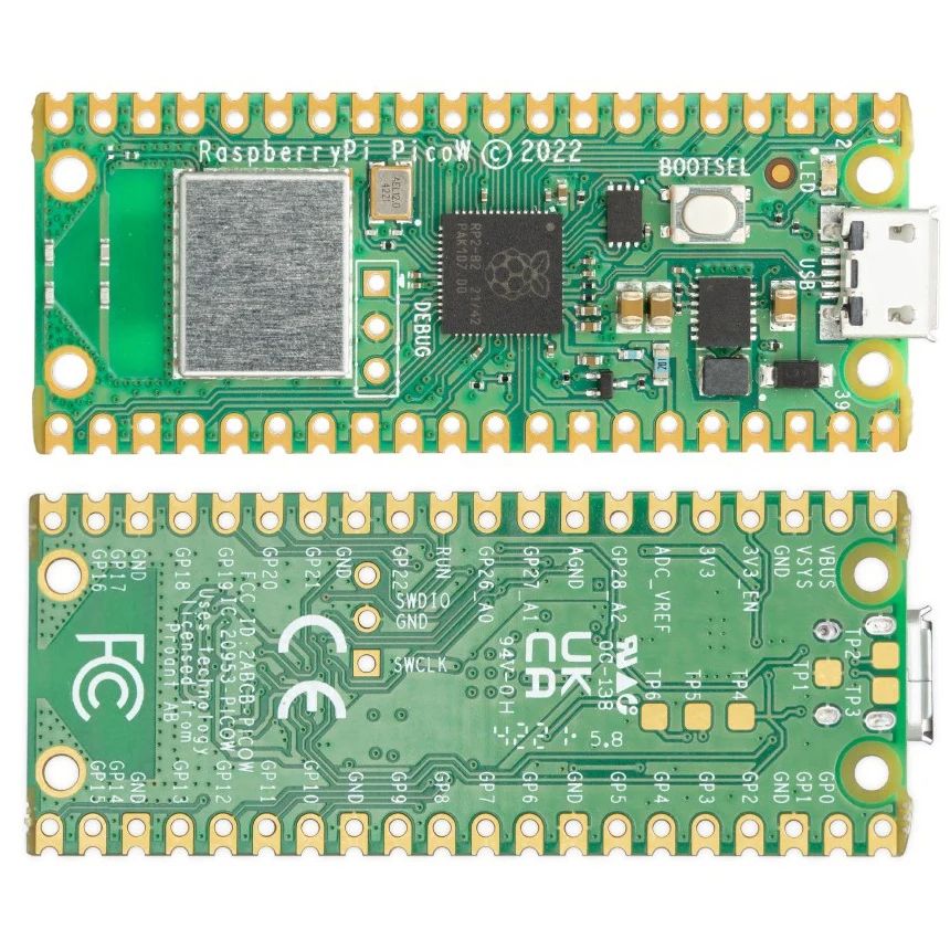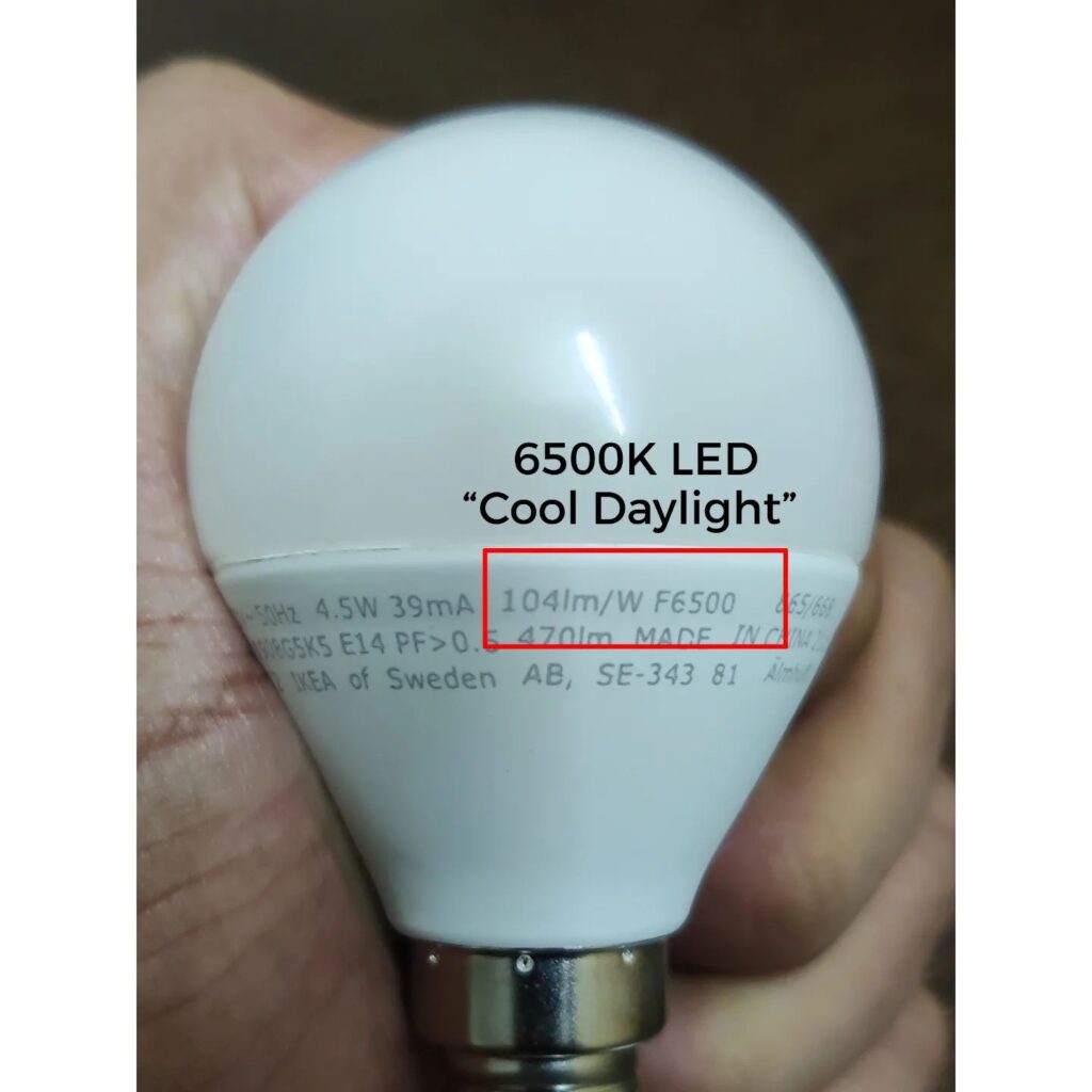
I am sure most folks when they are picking out what LED bulbs, usually buy LEDs by colour and go via marketing jargons like Warm White, Cool Day, Warm Yellow etc. These terms usually represent the output colour of your LEDs. Some of you would know that there is a standard way to represent them in terms of colour temperature with units in Kelvin(These would be mentioned on your bulbs). Let’s explore what those are today.
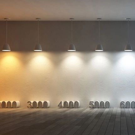
The temperature of colour is a weird way to represent information. Colour has no “heat”. So why use temperature as a measurement unit for it? It all goes back to a concept known as a black body radiator. In simple terms, it’s a theoretical material which emits radiation(aka light) when heated to different high temperatures. For example, think of a metal(which is a somewhat close real-life black body), when it’s heated to say 1500K has a particular glow in the red/orange range. Now when you start increasing the temperature of this material, the colour slowly starts to change white(Bluish tinge). So hence temperature Kelvin is used in relation to the colour of light. The temperature range can go from 1500K – 10,000K+. 1700K range corresponds to candle-flame-orange light & 6500K is clear sunlight on a bright day. So you have a huge range of LEDs to choose from based on what you want.
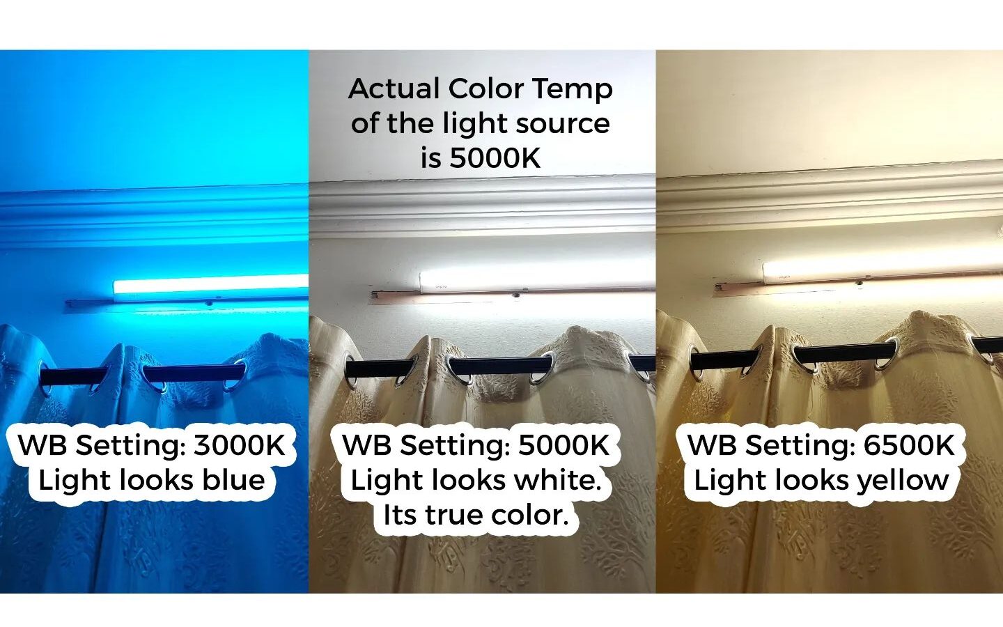
Now let’s come to photography of this light. Where it’s all relative to your settings. Open your mobile camera and go to the manual mode in your camera you will see there is something known as White Balance on the settings, This is also measured in Kelvin. This setting is telling your camera sensor what pure white light is. Let’s say you put the WB setting on the camera as 5000K and take a photo of an object. So any light source in your scene with a colour temp of 5000K will appear white on your image whereas any light source lesser than that will appear Yellow and anything above will appear bluish. It’s as simple as that. Now if slide up your white balance to say 6500K setting you will see more things looking yellow (if the scene lighting is at say 5000K). Knowing this concept will help you take killer pics and set the lighting mood for your camera. Take a look at the picture for seeing how an image will come out for the same lighting scene shot with different WB settings.