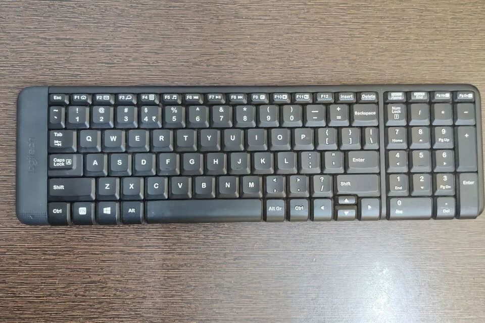
Had an external Logitech Keyboard stored away in a box. Alas, I left the batteries on them! It leaked to spring contacts and then the circuit. It has corroded a whole most of the Carbon and Copper pads on the circuit. It’s beyond repair and it’s officially dead.
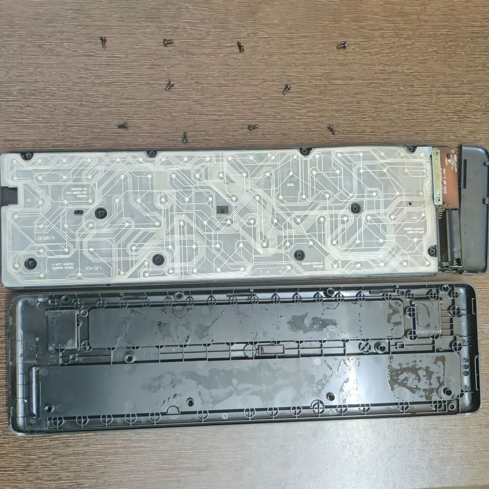
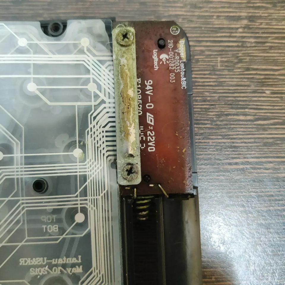
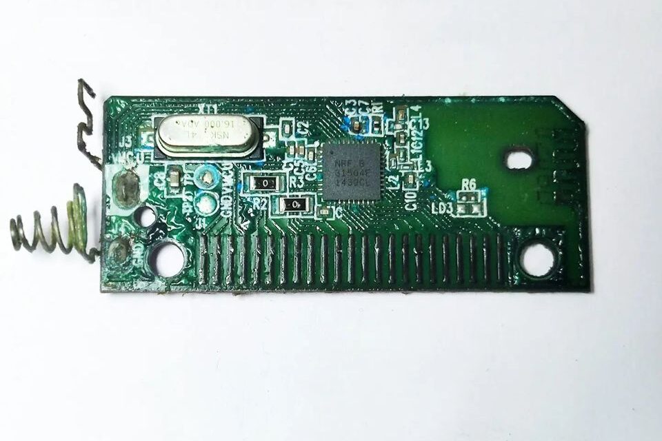
Coming to the teardown, the internals of most keyboards (Non-mechanical switch type) will contain multi-layer plastic sheets with printed silver contacts acting as switches. When you press down, the 2 layers come in contact and a press is registered. It’s usually wired in a row/column approach and it’s polled many times a second to register a press. These sheets are press fitted on Carbon contacts on the main PCB. Carbon contacts are a cheap and reliable way to avoid physical connectors. In the image, you will see them as black fingers on the edge of the PCB. These are driven by Nordic’s old nRF31504 2.4GHz Wireless IC. It has a PCB antenna which communicates to your PC via a 2.4GHz dongle. Few PCB traces are all corroded by the battery leakage. The metal can is a 16MHz external crystal to maintain timing for the chip. It’s a shame that I couldn’t get this working.
Let’s talk batteries now. Why do Alkaline batteries leak? Usually, when left on a product for a long time, the battery discharges and a chemical reaction causes the generation of hydrogen gas, which can break the seal even in good brand batteries. Once the seal is broken, the alkaline electrolyte Potassium hydroxide leaks onto the contacts and it reacts with Carbon dioxide in the air to form your white powder (Potassium Carbonate) which you find on the metal spring contacts. KOH is highly corrosive and it eats away your copper traces. So never keep batteries in your product if you are not going to use them.
Pro Tip: If you have a problem like this and the leakage hasn’t affected the circuit, you can use any mild acid like vinegar to clean those metal contacts and neutralise the white powder and get your device working.