Flipped Capacitors

Different Capacitor Shapes

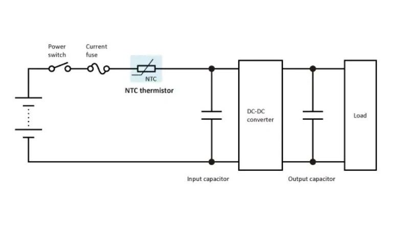
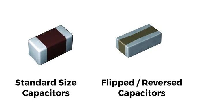
Most electronic design engineers know SMD capacitor parts come in the “standard” sizes of let’s say 1206, 0805, 0603,0402, 0201 etc. The common element of these parts is that their size is longer along terminals(between 2 pads you actually solder) than along the width of the part. Most times width of the part is half the length. There is a different class of capacitors which are wider than long. These are called flipped or reverse geometry capacitors. So the sizes will be 0612, 0508, 0306, 0204 etc. (To be honest, you might not find a flipped capacitor for every “standard” size capacitor though)

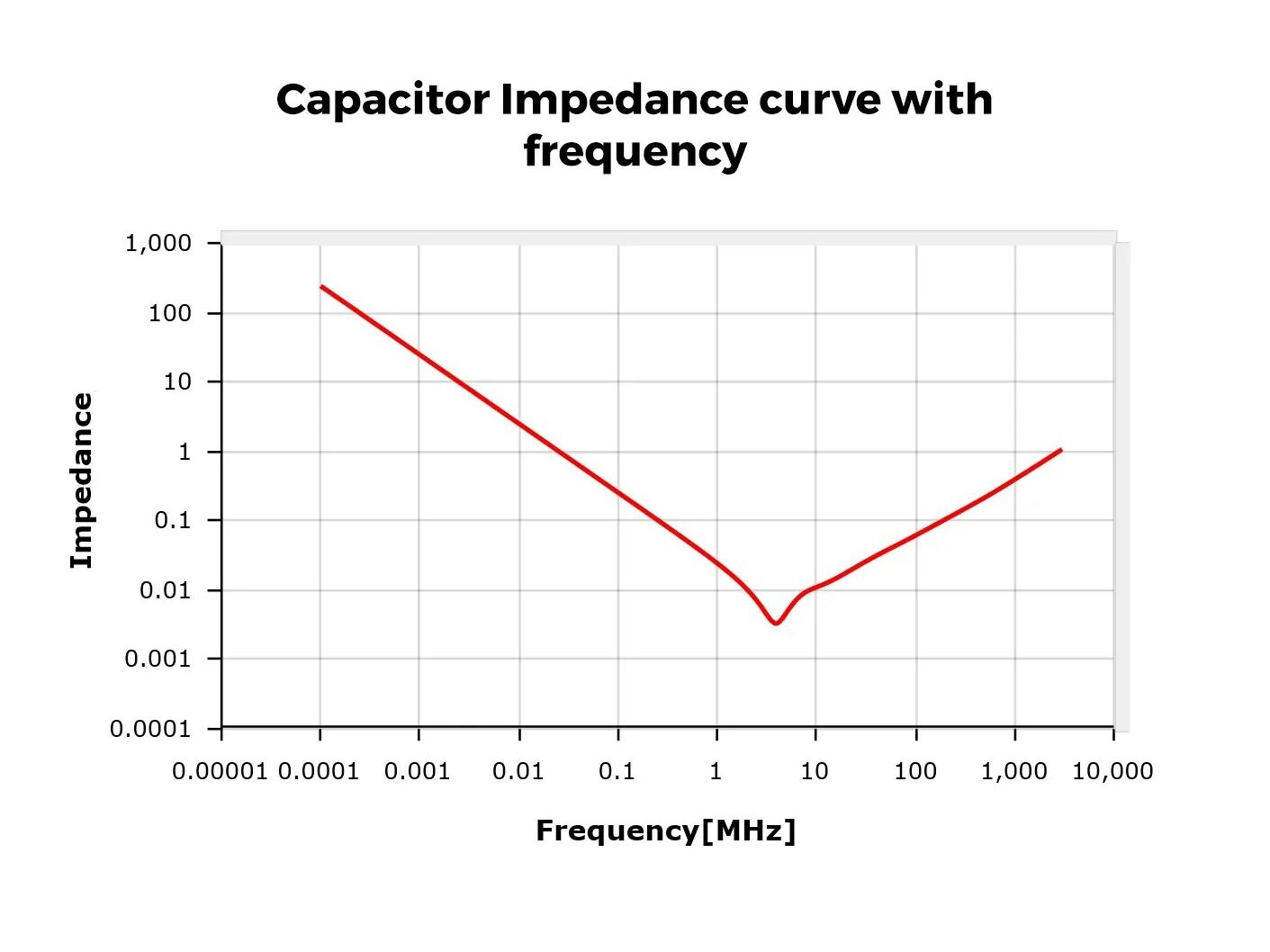
Why do we want to use a flipped capacitor? In one of my older posts, I explained that a capacitor in real life is not a capacitor by itself. It has an equivalent series resistance(ESR) and inductance(ESL). For an ideal capacitor, we would want to have ESRs and ESLs to be zero. Since there is an ESL in a capacitor, you usually see a V-shaped impedance curve with frequency in capacitor datasheets. The impedance value keeps getting low till a point and then it increases due to ESL. Here is where flipped capacitors come into the picture. Flipped capacitors are designed specifically to reduce ESL. When you flip the width and length dimensions of a capacitor, it reduces the soldering pad distances(or the length). Lower travel length means lower inductance and lower conductor length(Not to complicate it more, loop area also reduces, which is a good thing). So current needs to travel a shorter distance. A wider flipped capacitor effectively can have an impedance curve which is similar to 3-4 same standard-size capacitors. That means overall lower BOM count and layout space is lesser. For these reasons, these wider capacitors are starting to gain acceptance in the PCB design space.

If you liked the post, Share it with your friends!

Back to Basics: Inrush Current Limiters

Inrush Resistors
Inrush Resistors

When designing circuits, one of the key elements that are missed by many designers is the addition of inrush current limiters because they are mostly unaware of its use case. Inrush current as the name implies, is a large flow of current at the power on of a device. When PCBs are designed, we do scatter decoupling and bulk capacitors around the entire board to maintain the power supply stability for individual ICs. There can be massive bulk capacitors which are used specifically in large current applications like motors, audio amplifiers etc. When power is off, think of these as massive empty tanks. When the power is turned ON, there will be a massive surge to fill up all these empty tanks and hence you can expect an order of magnitude of instantaneous current flow in the circuit. So why is this large rush a problem? The large draw will immediately collapse your input power rail momentarily by a big factor, now if components of your circuit are not resilient to these power supply changes it can damage parts or may cause temporary glitches at the startup which may not initially be obvious. Even a load capacitance of 100uF can generate a 6.88A of inrush current which can cause a supply rail to drop 3.3V to 960mV. So it’s not something which can be ignored.

You can fix this by adding two things to your circuit, one is an integrated load switch with an adjustable slew rate which limits the rate of current draw for the downstream components. Adjusting the rate drastically reduces the inrush currents. The second method is the one which you see in most circuits is to use NTC thermistors as limiters. Connected in series, these have high resistance when starting off and as soon as current starts flowing, it heats up and the resistance drops to let more current through. So you effectively slow down the inrush requirement. Both have their pros and cons, so next time do check out the need for these in your circuits while building them.

If you liked the post, Share it with your friends!
1 56 57 58 59 60 66