I found this while browsing the interwebs and thought it’s cool enough to do a small post. It’s a reasonably big deal, no-one seems to be discussing much on.
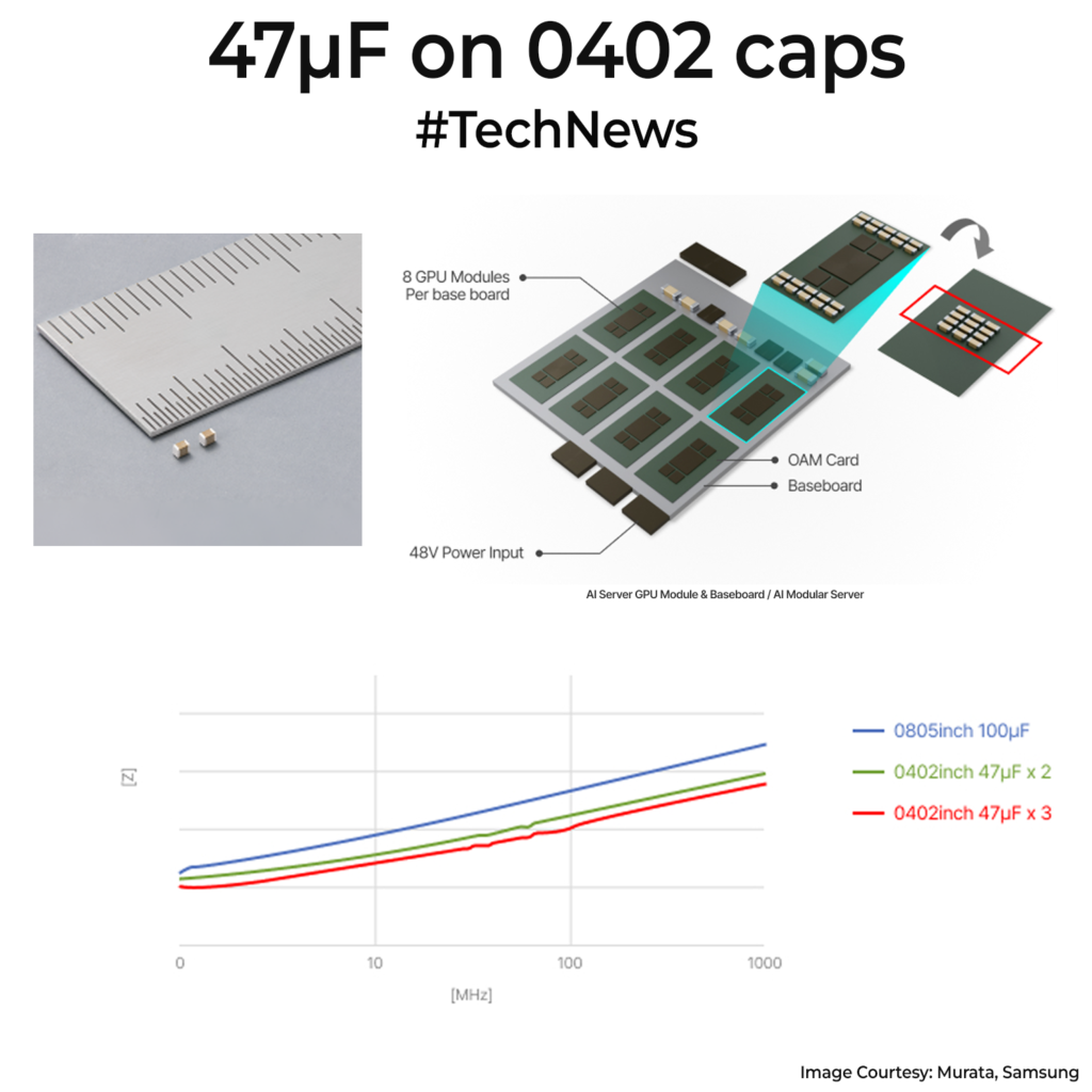
When selecting decoupling capacitors, you would ideally want to have the largest capacitor value in the smallest form factor to keep ESL/ESR in check. Capacitor manufacturer Murata claims that they have started the production of 47µF capacitors on a 0402 form factor(1mm x 0.5mm) design. Usually you don’t get these very large capacitor values in these small sizes. I am also hearing that, Samsung and Kyocera also have made the same 47µF in the 0402, but they in early R&D and production slated to start later this year.Previous largest in the same size was 22µF.
Why this matters is cap placement. 0402 lets you put serious capacitance values right next to power pins and BGA breakouts, which cuts loop inductance drastically. This means the Power Delivery Network is stable with these capacitors acting as the local energy reservoirs. Expect roughly 60% less mounting area than a 47µF 0603 part. This means you can have multiple of these caps in the same area. Meaning in phones, wearables, and AI server boards, around VRMs and GPU substrates, tighter placement can replace a chunk of mid-bulk caps and reduce the number of vias to ground.
Murata caps seem to be X5R Class-II type with a rated voltage of 2.5V. So these are good for only 0.7 – 1.8 V rails. But the problem can be the DC bias. At the actual full DC voltage, capacitor value will be much lower as it’s a Class-II ceramic material. I tried to see if there are charts on Murata Simsurf tool, but they don’t seem to list these latest caps. So we need to wait till those are available for the general public.
But this is a good sign anyway. We will have the possibility of much bigger capacity caps for strong decoupling pretty soon. Keep a lookout for these in the future board designs.
Part Numbers: GRM158R60E476ME01D, CL05X476MS6N9W