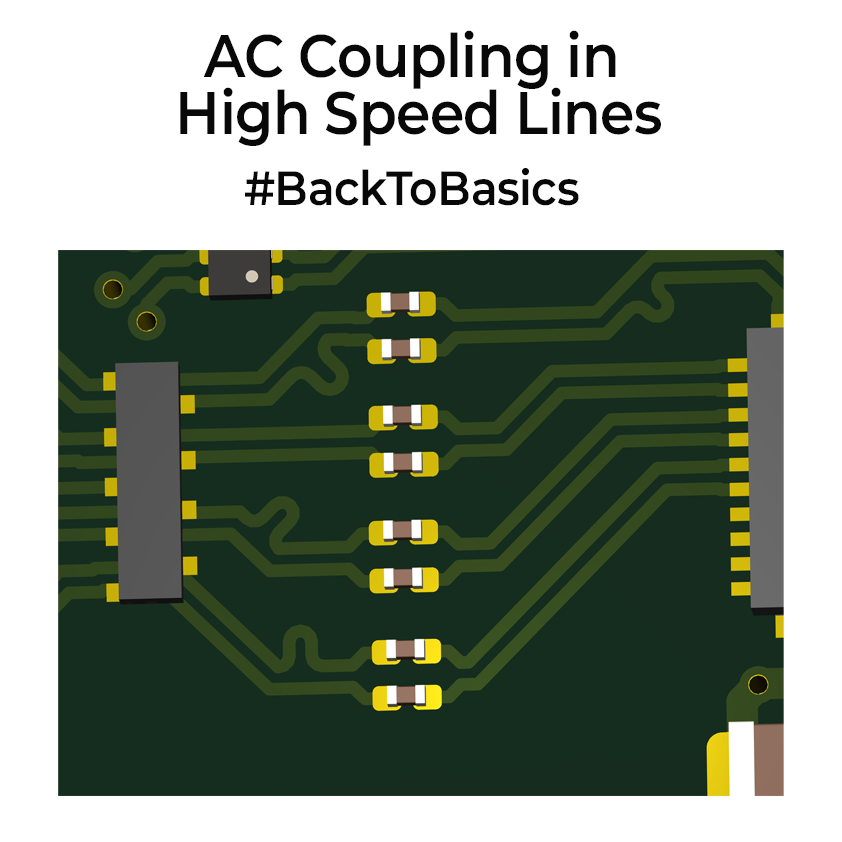
Back to Basics: Copper Thieving

Some of you might have seen these in PCBs. Let’s discuss in detail today.

Copper Thieving

In PCB manufacturing, during the final plating, the bare panel sits in an acid bath and a direct current pushes coats Copper on every exposed metal area on the PCB. Pads, vias and any existing copper act like little magnets. Areas that already have a lot of copper pull harder, empty laminate pulls less. Thick spots get thicker, thin spots remain thin. This is a problem in some cases like the via holes where you will have thickness difference, which in turn can cause signal integrity issues when high speed signals travel through them.

Copper thieving is done to fix this issue. Designers/Manufacturers put small, unconnected dots or rectangles into the blank places on the outer layers of the PCB. These islands are supposed to “steal” a part of the current from certain regions. Current density flattens out, so the whole panel plates at the same pace. This means uniform via walls and traces etch to the correct width/depth.

Do not confuse thieving with copper balancing, though. Balancing is a layout stage move where you mirror large ground pours across all layers so the stack-up expands and cools evenly during lamination and soldering. Thieving lives only on the two plated outer layer (inner layers are etched, not electro-plated). Balancing protects the overall PCB structure and prevents wrapage, while thieving is about fine-tuning in certain surface regions.

If you implement thieving, please remember to keep these islands some distance away from pads/high speed traces or antennas as they are usually not connected to avoid any unwanted coupling. Some folks do connect it to the ground layer with a few vias. So next time when you see some pretty rectangle islands or dots in the design, you will know it’s not there only for making it look nice, they do it to improve the manufacturing yield of PCBs.

If you liked the post, Share it with your friends!

Advanced Tech: AiC and AiP

Antennas have been the driving force of the modern wireless industry for a long time, especially the antennas on PCBs. Microstrip patches, slot antennas, and F-antennas printed on substrates like FR4 give us reliable performance below 30 GHz. They let us tune frequency by adjusting patch dimensions and feed geometry. When we push into bands above 30 GHz, losses from copper roughness, substrate modes, and dielectric loss make PCB antennas inefficient and bulky.

To overcome the limits of PCB antennas, we are moving into two new approaches: Antenna-in-Package (AiP) and Antenna-in-Chip (AiC). In AiP, think of the antenna as part of the chip’s casing. It’s a miniature multi-layer printed-circuit board that just happens to have a bare RF chip solder-bumped into its centre and then gets shipped as a single surface-mount part. By printing or mounting the radiator onto the package substrate using low-loss organic laminates or ceramics, we ensure the materials do not absorb the signal. This lets us build small beam forming arrays and pack amplifiers, filters, and phase shifters right into the module.

AiC takes the idea all the way onto the silicon die. Here, we etch antenna shapes into the top metal layer of a CMOS chip. I’ve seen designers thicken that metal, add patterned ground shields beneath it, or insert artificial magnetic conductors to bounce more energy out of the lossy silicon. Some even place a thin cover (a superstrate) above the chip to help steer or focus the beam. Since silicon has a high permittivity and loses energy, it can’t get more efficient than a certain point.

AiC is an ultimate miniaturisation play, and AiP is the performance play. If you’re designing a smartphone or radar sensor today, AiP is the practical path, it gives you gain, beam-forming head-room and a cleaner PCB layout. You only pick AiC when absolute footprint has to be the size of the silicon itself, and you are pushing beyond 100GHz where antenna is only a few hundred microns long and PCB interconnects become impractical. To date, only a handful of functional antenna-on-chip prototypes have been demonstrated.

If you liked the post, Share it with your friends!
1 5 6 7 8 9 86